Automated optical inspection helps detect and classify defects and facilitates an efficient repair process.
Amir Peled and Ofer Saphier, Orbotech Ltd.
As thin-film transistor LCD panel makers produce increasingly larger televisions, fewer displays fit onto the glass substrate during the production process. Whereas fifteen 32-in.-wide displays fit onto an eighth-generation substrate, only six 52-in.-wide displays fit onto the same glass. The yield loss as a result of fatal defects is far greater for the substrate with the 52-in. screens.
Many of these defects, however, can be repaired. Thin-film transistor array repair systems have been widely adopted and are used to cut “shorts” (unintentional connections between conductive lines), repair “opens” (gaps in conductive lines) and weld conductive lines.
Repair is a mostly manual, time-intensive process that requires an operator to review each defect, determine its repair parameters, execute the repair and examine the outcome. For efficiency, automated inspection and testing are essential in identifying repairable defects. Go/No-Go inspection and testing methods are performed on all samples to determine whether a panel or substrate should enter the next process step or be repaired, reworked or scrapped.
Automated optical inspection systems scan the substrates at various stages of the thin-film transistor array production process. They use multiple CCD cameras, advanced illumination techniques and special algorithms to detect defects early on in production.
For example, in eighth-generation fabrications, automated optical inspection systems are required to scan an area of more than 5 m2 (53.8 sq ft) and to report defects of 5 μm or less, with a total average cycle time of less than 60 seconds. Repeat patterns of pixels across the panel enable cell-to-cell comparison to identify abnormalities by comparing gray levels captured in the camera with those of neighboring cells. After the defects have been located, a microscope captures high-resolution color images of them.
The images are sent to a computer for automatic classification of defects using machine vision techniques.
The process can be challenged if the number of defects is large. In many cases, especially with in-line inspection, the microscope cannot capture all defects within the desired total average cycle time. To solve this, methods for filtering insignificant defects are required. In today’s most advanced automated optical inspection systems, manufacturers use a combination of filtering methods during the initial scan stage. Only defects that pass through these filters require further microscopic analysis.
The filters are based on certain features extracted from the defect (size, gray levels, location, etc.) as well as on comparing coordinates to defects found in earlier inspections. The results are available after scanning and are used primarily to filter out noncritical defects and determine those that require more accurate video review and classification. The last stage in defect classification is also the most precise. A high-quality three-chip CCD camera using various types of illumination captures more detailed images of the defect, identifying its dimensions, color, size, location and other criteria.
For example, dark-field illumination — capturing scattered light — helps to distinguish between nuisance particles and repairable defects (Figure 1). More than 100 features of the defect are extracted from the images. These features identify its dimensions, color, size, location and many other criteria.
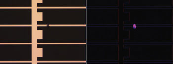
Figure 1. Dark-field illumination is shown here using directional multicolor illumination to distinguish between “open” and dust defects (patent pending). Because of strong light scattering, both types of defects appear as dark spots in conventional bright-field illumination (left.) The brightness of an “open” defect is very sensitive to the direction of illumination, whereas dust defects appear bright, regardless of the direction of the dark-field illumination (right).
A classification engine processes the data and determines first whether a defect can be repaired and, if so, what type of repair is required. Two of the leading automatic classification approaches are learn- and rule-based.
Classification methods
In learn-based classification, the machine-learning system uses a collection of sample images already sorted into classes to learn the optimal separators (hyperplanes) between classes in the feature space, after which any new defect can be automatically classified. Feature space is a mathematical term for a multidimensional space in which each dimension is a feature, for example, a 2-D space in which X represents the size, and Y represents the brightness of the defects.
This method simplifies the setting of classification criteria. Employing a “hints” function that suggests which features to apply, users can insert guidelines into the learn-based engine to include or ignore specific separators; e.g., to ignore the size of the defect but consider its color for classification. Learn-based classification is used where either the cell structure or the defects are more complex and when enough samples are collected.
Rule-based classification is the process of classifying defects by using a set of preliminary rules defined by the user. The rules are based on a set of known features. The method is most effective during ramp-up, when manufacturing a new device with rare types of defects, or when the production process/recipe frequently changes.
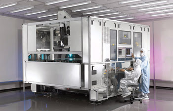
Figure 2. The SuperVision automated optical inspection system, one in a series of off-line and in-line inspection systems produced by Orbotech, is designed to improve production yields. It offers defect sensitivity as high as 1.5 μm as well as advanced defect classification for sixth- to eighth-generation glass sizes.
Results gathered from actual production indicate that both classifications should be used to support efficient repair decisions along the product life cycle. In this price-sensitive and cost-competitive market, where material costs are high and account for a large percentage of the total panel cost for larger displays, it is critical for manufacturers to constantly strive toward maintaining the highest possible yields. Leading automated optical inspection systems deliver yield enhancement solutions and defect classification capabilities that maintain yields and improve productivity and product quality.
Meet the authors
Amir Peled is a product marketing manager at Orbotech Ltd. in Yavne, Israel; e-mail: [email protected].
Ofer Saphier is an algorithms and feasibility manager at Orbotech Ltd.; e-mail: [email protected].