Applying microelectronics techniques to optics enables economies of scale for next-generation phones.
Michael Feldman, Tessera North America
Wafer-level optics is a novel technology that is designed to meet the demand for smaller form factors, higher resolution and cost-effective pricing in the next generation of camera phones. The optical components are fabricated on glass wafers in a manner similar to that of fabricating integrated-circuit chips on silicon wafers. The entire camera is aligned and assembled at the wafer level and subsequently diced to form individual camera modules.
The size of a camera module, often the largest component on a board, is a primary factor limiting handset design. Ideally, the camera would be located in the lid of a clamshell design. However, current handset designs often place the camera in the hinge of the phone (Figure 1); otherwise, the camera is limited to VGA resolution (640 × 480) to allow it to fit within the lid.
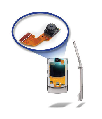
Figure 1. Contemporary cameras are located in the hinge of the mobile handset.
Cameras in phones also require special handling. Camera modules are thicker than integrated circuits and cannot be attached using the same solder reflow process used on the circuits because of the temperature extremes encountered during reflow. Thus, the cameras are typically attached with a socket or are wire-bonded to a separate thin, flexible circuit, which is attached to a connector that is bonded to the board during the reflow process. Wafer-level optics manufacturing solves many of these size and assembly issues.
Camera lens formation
Instead of using conventional molding techniques to form individual lens elements, makers create wafer-level lens surfaces using wafers of transparent material. The two primary approaches to forming lenses on the wafer surfaces are direct-etch and replication.
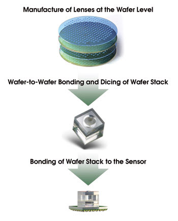
Figure 2. This illustration shows the wafer-level camera fabrication and assembly process that creates extremely thin camera modules.
The direct-etch method consists of patterning a resist on a wafer with conventional semiconductor lithographic techniques. The resist is then reflowed to form hemispherical shapes, and the wafers are dry-etched, transforming the hemispherical resist shape into the wafer material.
In the replication method, a master wafer is created as a mold. A replication material polymer is deposited on one or both sides of the transparent wafer, and the master wafer is brought into contact with the replication material, which is cured, thus forming the lens surface.
After lens formation, multiple lens wafers are bonded together to form a wafer stack. Alignment marks typically are placed on each wafer with conventional photolithography tools, and a UV or thermally cured adhesive is used for bonding.
Alignment requirements are dictated primarily by the lens system design, and typical tolerances range from 5 to 25 μm per wafer. However, with tighter alignment tolerances, manufacturers can improve design performance.
Wafer-level alignment also enables the use of precision alignment techniques, which help maintain performance levels and reduce manufacturing costs. With conventional camera technology, each lens system is assembled individually. It becomes difficult and expensive to achieve alignment that falls in the tighter portion of the expected range. This limits performance and increases the variability from part to part.
Once the optical element is ready, it is bonded to the package sensor, thus creating the camera module. Because the active sensor area is significantly smaller than the image sensor chip, it is advantageous to dice the lens wafer stack and individually bond each lens element to the package sensors. It allows a greater number of lens dies to be incorporated onto each wafer, and it allows greater throughput.
The camera lens height can be achieved through a variety of methods, including Tessera’s Shellcase RT technology, in which the sensor is packaged using a cover glass and electrically connected with a ball grid array. Once assembled, the wafer-level camera can be attached directly to a printed circuit board, leveraging the same reflow process used to attach the integrated circuits to the cell phone board, while eliminating the need for a lens barrel, plastic lens holder, flex lead and connector.
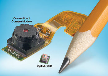
Figure 3. A prototype wafer-level camera module recently developed at Tessera is compared with a conventional cell phone camera.
Technology demonstrator
Besides reducing the amount of labor required, the number of components required to build the camera is reduced. As a result, a VGA wafer-level camera is significantly smaller than a conventional VGA camera (Figure 3).
By enlisting existing manufacturing and assembly processes used by the semiconductor industry, wafer-level camera technology can reach the economies of scale required to achieve the very small form factor and high resolution needed for next-generation camera phones.
Meet the author
Michael Feldman is chief technology officer for optics at Tessera North America in Charlotte, N.C.; e-mail: [email protected].