Explosive growth of mobile imaging leads vendors to seek new designs.
Vladimir Koifman, Dr. Gershon Rosenblum and Arie Gavriely, Advasense Technologies Ltd.
The burgeoning camera phone market is creating a growing need for very compact high-megapixel sensors. Highly shrunken pixel designs for such sensors present challenges such as reducing pixel crosstalk and color disparity, eliminating image lag and noise, and increasing light sensitivity and well capacity.
If you point a mobile phone camera at a uniformly illuminated white surface such as a wall or a sheet of paper, chances are the image will have areas tinted by pink or perhaps cream or green. Because the color and shape of these areas change for various illumination types or color temperatures, it is difficult to fully suppress the tints by image signal processing. Although we are most sensitive to minute changes in white, gray or skin colors, the effect is similar with other colors. In fact, actual color representation errors may be greater for saturated colors.
These color errors are caused mainly by color crosstalk, an effect of colors mixing in the camera. For example, red light might contribute to the signal of green pixels. Crosstalk requires an image signal processing color-correction algorithm to restore the correct colors in the image, which increases noise levels. Thus, color speckle and other noise, especially visible on dark imaged surfaces and at low illuminations, also are indirect results of crosstalk.
Crosstalk occurs because in digital photography, in contrast to film, separation of the colors of light and the actual sensing occur in different points of the sensor and at significant distances from each other. In CMOS image sensors, incoming photons go through color filters, then through glass layers supporting the metal interconnect layers, and then into silicon, where they are absorbed, exciting electrons that then travel to photodiode structures to be stored as signal. Along the way, the photons and electrons have many opportunities to be diverted and end up at the wrong photodiodes, contributing to the wrong color signal.
Often, crosstalk is referred to as either optical or electrical, depending on whether photons or electrons were diverted. However, this differentiation is difficult to measure, so it seems more practical to classify optical crosstalk as the part that can be reduced by pixel structure changes above the silicon-glass surface; electrical crosstalk is the part affected by changes in the structure and voltages inside the silicon. More “electrical” crosstalk may result from electric field interaction between the photodiodes through the signal integration time or during readout. The incomplete color separation by the filters often is referred to as spectral crosstalk.
As market pressure drives down the pixel size in cell phone cameras, the optical crosstalk problem becomes more severe because the decrease in pixel pitch separates light of different colors on an ever smaller scale. A CMOS image sensor photodiode typically occupies 20 to 40 percent of the pixel silicon surface area because of the need to accommodate pixel transistors. The photodiode-to-pixel area ratio is called the fill factor.
The microlens originally was introduced to improve the sensitivity of a sensor by directing more light from the pixel periphery toward the photodiode, thus increasing the “effective fill factor” — the fraction of light that hits the silicon on or close to the photodiode and thus has a chance to contribute to the signal. By the same token, a microlens may reduce the amount of light that hits a photodiode after crossing a filter associated with its neighbor.
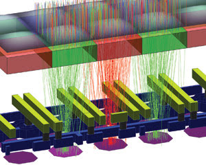
Figure 1. This ray-tracing scheme shows the structure layers of a CMOS. From top to bottom, the layers are microlenses, color filters, “metal 2” lines, “metal 1” lines and photodiodes.
The microlens and crosstalk
A pixel ray-tracing scheme might make it appear that a well-designed and well-controlled microlens can all but eliminate optical crosstalk. However, the ray-tracing approach to light propagation, although intuitive, works well only for structures much larger than the light wavelength. It becomes grossly inaccurate in small pixels (of pitch below 3 μm) in which the structure details’ sizes are of the order of the visible light wavelengths of 0.4 to 0.7 μm. The minimum spot size to which the light can be focused by an ideally shaped microlens is limited by diffraction to a value close to λ*h/p, where λ is the wavelength, p is the pixel pitch and h is the height between the silicon top surface and the microlens bottom surface. The pixel’s height-to-pitch ratio is called the pixel aspect ratio, and reducing this ratio is a major goal of CMOS image sensor technologists.
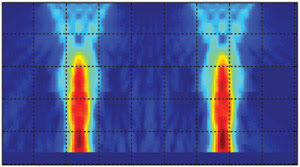
Figure 2. This example of frequency domain-time domain simulation shows results of light propagation inside a small pixel. The brighter color represents higher color intensity.
A microlens shape close to optimum focuses light into a spot on the photodiode. The spot shape can be mapped by a two-dimensional bell-shaped curve when the spot size is close to the diffraction limit. Because the spot periphery is close to the neighboring photodiodes, the light there contributes to crosstalk. Therefore, the amount of crosstalk depends crucially on spot size, and it is strongly affected by the microlens shape. Any deviation from the ideal size or shape increases crosstalk. In addition, microlens formation process control — as well as process stability — is important because variation in crosstalk between different sensors is difficult to account for in image signal processing.
One problem with microlenses is that some of the light can enter gaps between the microlenses and be scattered by the irregular concave surfaces. This light contributes a lot to color crosstalk and almost nothing to sensitivity. Thus, those working with microlenses want to reduce this gap area.
Other than microlenses, other factors can contribute to crosstalk. For example, crosstalk can be increased (and sensitivity lowered) because the light passage in the interconnect glass is curved by diffraction and by scattering around the absorbing-reflecting metal lines and vias. Traditional pixel design pushes the lines as far as possible outside the photodiode into the pixel periphery to minimize their optical influence. However, increasing some linewidths can help reduce crosstalk by creating a shielding effect around the photodiode that lets light from the correct color filter through but blocks light crossing from a neighboring filter. If this metal shielding design is used, it should balance the crosstalk decrease with the inevitable sensitivity decrease.
Reducing the aspect ratio for a given pixel pitch means that the interconnect stack height and color filter heights also are reduced. Reducing the color filter height should be balanced against increasing the spectral crosstalk. A thinner green filter would allow more red light through, so an increase in absorptivity of the filters’ material is required to achieve the height reduction.
The interconnect stack holds the metal interconnect layers. Reduction in height of each layer should be balanced against increases in the metal lines’ resistivity and cross-capacitance between the lines in various layers. Reducing the number of layers is a major goal of the CMOS image sensor design.
The newest CMOS image sensors have a pixel pitch of 1.75 and 2.25 μm, are designed with two or three metal interconnect layers (versus three to five layers in the older 3.5- to 6.0-μm pixel sensors), and have an aspect ratio of approximately two. These characteristics produce an acceptable final image color quality. However, it must be reduced further for even smaller pixels to become viable. The reduction in pixel size with no image color quality deterioration is becoming ever more difficult as the light is being pushed into photodiodes that are smaller and spaced closer than the wavelength itself.
Straining pixel design
One main target in small pixel design is to increase the photodiode area, because a larger photodiode improves light collection efficiency even when light spot size is large and because a larger photodiode can collect more electrons, increasing the full-scale signal (one of the most important pixel parameters).
Naturally, if the photodiode area becomes larger, the area for all other components becomes smaller. A typical four-transistor pixel contains four metal-oxide semiconductor transistors in addition to the photodiode. Once pixel size shrinks, it becomes nearly impossible to place four transistors inside each pixel. Therefore, most small-pixel image sensors use sharing, where some of the transistors are shared between pixels. In shared pixels, each photodiode has its own transfer gate, while other transistors are made common for neighboring pixels. The most typical method is to share transistors between two or four pixels, giving an effective number of transistors of only 1.75 or 1.5 per pixel, respectively.
Minimizing crosstalk is important in the electrical portion of pixel design, too. Ideally, each absorbed photon should generate one photoelectron in the closest photodiode. In practice, some photoelectrons find their way into the neighboring pixels. To prevent this, pixel designers try to optimize the size of the photodiodes as well as the distance between them. Also, additional implants can be used to create diffusion barriers between photodiodes.
All this requires a freedom to manipulate the photodiode’s physical design and related manufacturing process. However, this is not always easy because the pinned photodiode used in modern four-transistor pixels is tightly integrated with the transfer gate to optimize its charge transfer efficiency. This optimization is the cornerstone of good four-transistor pixel design.
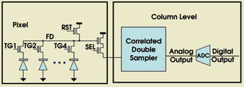
Figure 3. This conventional four-transistor (4T) pixel readout is a four-pixel shared design. Each photodiode has a transfer gate transistor (TG1-TG4). The correlated double sampling readout relies on a complete charge transfer from photodiode to floating diffusion node (FD). If the charge transfer is incomplete, the pixel suffers from image lag (ADC = analog-digital converter, RST = reset, SEL = select).
The four-transistor pixel design is based on a correlated double-sampling technique (Figure 3). During signal readout, the floating diffusion node is sampled twice: first, with transfer gate off, then again when the photodiode charge is transferred to floating diffusion node. It is of utmost importance to transfer the photodiode charge completely so that there is no charge remaining on the photodiode at the end of charge transfer phase. Any residual charge on the photodiode causes image lag and excessive noise. Most of these problems are especially evident at low illumination levels.
A 1.75-μm pixel in a modern image sensor might get only 30 to 100 electrons of photosignal for images taken with 100-lx illumination. If the charge transfer is incomplete and leaves just 30 electrons on the photodiode, a major image lag in the sensor results. What’s more, the 30 electrons left are usually noisy and change from pixel to pixel.
This is why pixel designers spend a lot of time trying to achieve a charge transfer as complete as possible. However, accomplishing a complete charge transfer often comes at the expense of other parameters such as full-well capacity — the maximum charge that a pixel can store and transfer for readout.
The larger the full-well capacity, the higher the sensor’s dynamic range is. For complete charge transfer, the photodiode volume should be fully depleted at 1 to 1.5 V. This means that the photodiode doping should be light, which means a low capacitance and a small full-well capacity as well.
To improve red color sensitivity, the photodiode junction must be placed deeper into the silicon. This deep photodiode must be doped less so that it depletes fully at 1 to 1.5 V, which results in a low full-well capacity.
Thus, low full-well capacity becomes the major problem in pixel scaling. Old 3.6-μm pixels often gave full-well capacity in excess of 30,000 electrons. However, scaling the pixels to 2.2 μm reduced full-well capacity to about 12,000 electrons. Generally, today’s 1.75-μm pixels have full-well capacity of less than 10,000 electrons.
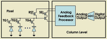
Figure 4. At first glance, the Advasense feedback-controlled pixel appears very similar to the four-transistor shared pixel. However, feedback takes care of any problems with incomplete charge transfer, so the photodiode and transfer gate transistor design become more relaxed, resulting in higher full-well capacity, lower crosstalk and better sensitivity.
The low full-well capacity problem can be solved by using feedback to reduce image lag and noise (Figure 4). Advasense’s feedback-controlled pixel does not require full charge transfer, as feedback ensures that image lag is virtually zero. The photodiode storage capability then can be greatly improved and pixel scaling simplified. With these and other innovations, the industry can continue pixel size scaling down to at least 0.9 to 1 μm.
Meet the authors
Vladimir Koifman is chief technology officer at Advasense Technologies (2004) Ltd. in Raanana, Israel; e-mail: [email protected].
Gershon Rosenblum is electro-optical group manager at Advasense; e-mail: [email protected].
Arie Gavriely is director of marketing and business development at Advasense; e-mail: [email protected].