Rapid laser patterning offers many advantages for manufacturing flat panel displays.
Matt Henry, Powerlase Ltd.
Flat panel displays are one of the great modern engineering success stories. They are everywhere — in mobile phones, public displays and even sports arenas. In fact, even now there is a fair chance that you use them every day at home, at work or both.
Patterning of thin films — that is, removal of parts of a thin film to create a desired pattern in the material that is left behind — is a crucial step in the manufacture of these displays. We have conducted extensive measurements comparing the conventional technique, chemical etching (i.e., lithography), with laser-based removal. These tests convince us that, in some cases, hundreds of millions of dollars can be saved by substituting laser patterning for chemical etching in the manufacture of flat panel displays.
If you have bought a monitor or a home television over the past few years, you know that the retail price of flat panel displays has fallen enormously. A 42-in. plasma-display television is perhaps one-third the cost it was two or three years ago.
To achieve such dramatic price reductions, manufacturers have looked to economies of scale, vertical integration and strategic partnerships for cost savings and for streamlined production. Competition is fierce among established companies for this lucrative market, and profit margins are often single-digit. In this most cutthroat market, new technologies that offer cost savings are eagerly sought. One such technique is the use of lasers to pattern thin films directly on glass.
Display architecture
There are three main flat panel display architectures: plasma, liquid crystal and organic LED displays. Plasma displays commonly are employed for large panels that measure 42 in. and above, and they are dominant for panels wider than 50 in., which are used both for home cinema and for public display information. LCDs are the most commonly employed design and are used in applications ranging from small cell phone displays to large-screen televisions. In the home television sector, plasmas and liquid crystals compete directly for screen sizes between 40 and 50 in.
Organic LEDs are a newer architecture that only recently has been brought to market by Samsung and Sony. Initially envisioned for mobile applications such as cell phones, mp3 players and notebook computers, this technology has potential picture-quality and energy-saving benefits that eventually may allow it to challenge liquid crystals as the mobile display of choice. But for now, because of the high cost, organic LEDs are restricted to high-end products.
Although widely differing in design, all three processes employ thin-film technology — specifically, nanometer-scale films that are deposited onto a substrate to achieve electrical and optical effects. Traditionally, such thin films have been patterned using wet-etch lithographic techniques, which have been utilized extensively in semiconductor manufacturing and which are well-qualified industrial processes. However, these architectures have drawbacks, particularly in terms of cost, where high chemical costs and low yields incur significant manufacturing overhead, especially for the manufacture of large flat panel displays.
Rapid laser patterning of thin films is an alternative to wet-etch lithography. Laser patterning employs a pulsed laser beam to ablate a thin film layer directly from a substrate. It is a noncontact, high-speed process that does not employ chemicals and that does not suffer from the low yields of lithography. Laser patterning is used commercially in the volume production of LCDs, and its use is growing. Its most conspicuous success is in the manufacture of plasma displays, where it has been employed for a number of years by some of the biggest plasma-display producers in the world, notably Samsung and LG.
To understand why laser processing has found acceptance in the manufacture of plasma displays, it is necessary to know a little about their operation. A plasma-display architecture has two separate structures: the substrate, which has rows of phosphors positioned above electrodes, and the glass superstrate, which has transparent indium tin oxide (ITO) electrodes that are orthogonal to those on the substrate1 (Figure 1). These electrodes are necessary to control each individual pixel on the display.
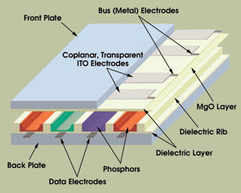
Figure 1. Indium tin oxide (ITO) electrodes are fabricated by selectively removing material from what was originally a uniform thin film covering the entire glass substrate.
The ITO is used on the superstrate because it is a transparent conductor; i.e., it is electrically conductive but also has a high transmission in the visible spectrum. Such unique properties mean that the ITO is used in almost all forms of flat panel display manufacture — whenever there is a need for transparent circuitry.
The ITO layer is coated uniformly onto the glass superstrate to a thickness of around 100 nm. The ITO then must be patterned to create the electrode array that enables address-ing of each pixel. Patterns vary by manufacturer but are always in a repeating structure. In Figure 2, you can see in an area that is 55 × 55 mm the pattern made of individual pixels, each created by a single laser pulse. Processing time for this region was on the order of 0.4 s. The pixels are an illustrative “T bar” electrode structure.
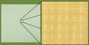
Figure 2. The pattern of ITO on a glass substrate is created by laser ablation.
The entire front panel of the plasma display must be patterned in this manner. Traditionally this would be achieved using a multistep wet-etch lithographic batch process. Using lasers to pattern thin films on transparent substrates is not a new idea: The process was discussed in research papers as long ago as the early 1990s.2 However, it is only in recent years that lasers able to pattern such large areas of glass fast enough for volume production have become available.
There are two key components to the success of laser patterning: the laser itself and its beam delivery system. The laser should be capable of kilowatt-level average power output at 1064 nm, with kilohertz repetition rates and pulse durations of tens of nanoseconds. Rugged diode-pumped solid-state lasers with fiber delivery options are the ideal candidates. Such lasers now are available with outputs of up to 1.6 kW of average power and pulse energies of 250 mJ, with pulse duration less than 40 ns, peak powers of greater than 10 MW and kilohertz repetition rates. These lasers are industrially proven with well over a million hours of use in 24/7 production environments with greater than 99 percent uptime.
Beam delivery
Such lasers typically produce outputs whose M2 beam quality is between 20 and 30, which is usually unsuitable for fine-focus applications, but that is where the beam-delivery system comes in. Optical design techniques more commonly associated with excimer lasers can be applied, making these lasers ideal for thin-film patterning.
In the Figure 3 schematic of a beam-delivery system, the incoming beam passes through a beam shaper to produce a uniform square or rectangular energy distribution at the mask plane, which then is demagnified and reimaged through a galvanometric scanner onto the substrate. The beam is rapidly scanned back and forth, with each pulse producing a pixel on the order of 1 mm2, so at kilohertz repetition rates, a large-area pattern can be built up rapidly.
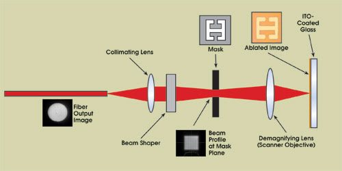
Figure 3. In laser patterning, an image of the mask is projected onto the substrate.
The key to this process is that the thin film must absorb the laser radiation more strongly than the substrate does. If this is the case, it is possible to remove the thin film selectively without damaging the substrate beneath. It is in essence a transmissive laser cleaning process, where the thin film is removed and any excess energy passes harmlessly through the substrate. For ITO on glass, the optimum wavelength is that of Nd:YAG — 1064 nm — which provides both excellent quality and fast processing rates. Extensive research into the precise mechanism of the removal of the thin film is ongoing; it has been demonstrated, however, that the process is thermal, with a high proportion of material removal by vaporization.3
Quality comparison
If a new technology is to displace a proven manufacturing technique, a detailed quality comparison must be carried out to ensure that the new process achieves or exceeds the quality standards of the established one.
We have made extensive measurements comparing laser patterning with the conventional chemical wet-etch technique.4 Starting with identical samples of ITO on glass substrates, we had one group of samples chemically etched by an experienced lithography company, and we laser-patterned another set in our laboratories. Then we tested both with a range of techniques, including scanning electron microscopy, energy-dispersive x-ray spectroscopy, atomic force microscopy, interferometry, optical microscopy and dark-field microscopy.
Our findings suggest that both processes remove the ITO thin film to an equal extent. Interferometric measurements indicate that the removal depth is within 1 nm for each process — better than the measurement error of the technique. As shown in Figure 4, energy-dispersive x-ray spectroscopy demonstrates that both processes remove the indium and tin spectral peaks characteristic of virgin ITO on glass, but that the elemental spectrum of the glass beneath otherwise is unchanged. This indicates that the ITO has been removed for both processes without affecting the substrate.
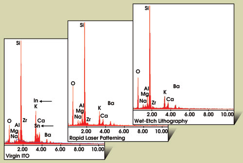
Figure 4. This energy-dispersive x-ray spectroscopy analysis indicates that conventional chemical wet etching and laser patterning are equally effective at removing ITO without affecting the glass substrate beneath it.
A significant concern is that the thermal nature of laser patterning could damage the glass substrate. Any glass damage during manufacture could lead to crack propagation and catastrophic failure of the TV during a plasma display’s projected 60,000-h lifetime. Dark-field microscopy will show any evidence of micrometer-scale glass cracking, but for both chemical etching and laser processing, there is no evidence of glass damage. Furthermore, we made interferometric measurements of surface roughness for both processes. We found no evidence of surface damage in the processed regions, the measured RA being 1.1 nm for wet etch and 1.3 nm for laser patterning — a roughness better than that of many optically polished surfaces and almost identical to that of the unprocessed glass.
In some ways, we found, laser patterning offers advantages over wet-etch lithography. Through comparison between interferometric and atomic force microscopic thin-film analysis, it becomes clear that ITO removal by wet etch is less consistent than laser patterning. Specifically, there is evidence of thin-film residue and of overetching of the ITO. Figure 5 shows a 3-D interferometric mapping of two comparative samples. Residue can be seen clearly for wet etch, while the laser-patterned sample is extremely consistent.
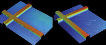
Figure 5. An angled interferometric comparison of rapid laser patterning (left) vs. wet-etch (right) samples.
Moreover, at the edges of the wet-etch sample, there are nicks into the side wall, known as “mouse bites.” (The laser-patterned sample shows spikes at the edges, but this is an artifact of the measurement resulting from the steeper sides of the laser-patterned sample.)
Wet-etch lithography is extremely sensitive to variations in thin-film thickness and glass topography, making it difficult to achieve consistent etching over a large area of glass. By comparison, laser patterning is an optical process that is effectively self-limiting with a liberal depth of focus — making it relatively insensitive to such variations. In both cases, edge resolution is on the order of microns, so it is possible to produce pixel sizes down to tens of microns. This is ideal for the production of the latest high-resolution plasma-display panel screens, which have a greater number of pixels for a given screen size. Full high-definition screens have 2 million pixels (1920 × 1080).
Cost comparison
The ultimate determinant between techniques is a detailed cost comparison for production volumes. Laser patterning has a number of compelling cost advantages over wet etching. The laser process requires only two processing stations — the laser-processing system and a water-rinsing stage. To achieve the same end result with chemical etching, between six and 10 processing stations are required. This means a much reduced footprint — particularly important because plasma displays are manufactured in cleanrooms, and large cleanrooms are very expensive.
Two of the primary cost drivers in lithography are the cost of chemicals and the low yield of the wet-etch process. Laser patterning is inherently nonchemical, removing that cost completely while making it far more environmentally friendly. And the high yield of laser patterning —better than 99 percent, compared with lithography’s 80 to 85 percent yield — gives laser patterning another strong cost advantage.
The initial cost of laser patterning equipment is higher, as are the maintenance costs for the lasers. However, Figure 6 shows the projected three-year total cost of ownership for a single production line producing 180,000 50-in. plasma displays each month from Gen 8 mother glass panels. The initial cost advantage of lithography disappears after 2 1/2 months, and laser patterning provides savings of up to $160 million over a three-year period. This equates to a $25 savings per television. These figures are taken from detailed end-user calculations and are a real cost model; however, their derivation is proprietary.
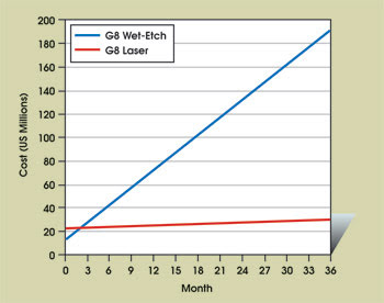
Figure 6. This chart shows the projected three-year total cost of ownership for comparable wet-etching and laser-patterning production lines. Although the initial cost of the laser system is greater, over a three-year period, a laser production line can save as much as $160 million.
This compelling cost advantage, coupled with good process quality and the desire for companies to use more “green” technologies, explains the success of laser patterning for plasma-display manufacture in the flat panel industry.
The laser patterning process does have some limitations at present, most notably in patterning multilayer thin-film structures, as found commonly in LCD designs, where it is necessary to selectively pattern thin films without affecting those beneath. The current laser patterning process employs an infrared wavelength, so there is significant energy transmission through the first thin film. This does not matter if the substrate is transparent and there is a single absorbing thin film; however, if there are multiple thin films, they will be vaporized together, making selective patterning impossible.
Research continues into solving this issue, with manufacturers seeking to produce high-average-power solid-state lasers at ultraviolet wavelengths. Such lasers have much shorter optical absorption depths, reducing energy transmission significantly and potentially solving this problem.
Limitations aside, laser patterning is not restricted to patterning ITO on glass. The laser process is well suited to patterning many thin films on various substrates, as well as metallic and even plastic films. This capability is of great interest in many other manufacturing applications; the cost of thin-film solar cells, for example, might be reduced dramatically if laser patterning were to replace lithography in their manufacture.
Meet the author
Matt Henry is the head of applications engineering at Powerlase Ltd. in Crawley, UK; e-mail: [email protected].
References
1. J.P. Boeuf (2003). Plasma display panels: physics, recent developments and key issues. JOURNAL OF PHYSICS D: APPLIED PHYSICS, pp. R53-R79.
2. J.G. Lunney et al (Aug. 5, 1991). Excimer laser etching of transparent conducting oxides. APPLIED PHYSICS LETTERS, pp. 647-649.
3. M. Henry et al (2006). Nanoscale analysis of laser ablated thin films used in industrial manufacturing of flat panel displays. Proceedings of The Laser Microfabrication Conference, ICALEO, Phoenix, pp. 188-197.
4. M. Henry et al (2007). Rapid laser patterning versus wet-etch lithography for flat panel display manufacture: a technical & commercial comparison. Proceedings of The Laser Microfabrication Conference, ICALEO, Orlando, Fla., pp. 119-128.