Laser processing can enable the production economies and increased device efficiency necessary for continued industry growth.
Finlay Colville and Corey Dunsky, Coherent Inc.
Despite its multibillion-dollar size, the solar industry exhibits many characteristics of an emerging sector in terms of manufacturing and product standardization. Indeed, rapid growth in solar cell manufacturing coupled with an extended period of consumer demand exceeding production output has left barely enough time for solar cell manufacturers and their equipment vendors to optimize existing production tools, never mind to agree on a common road map for the industry.
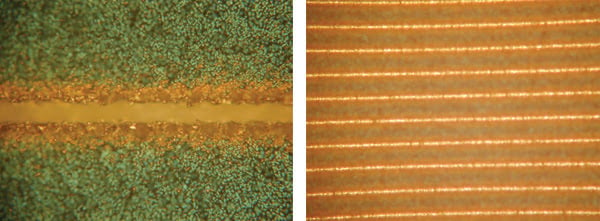
Front-surface scribing on a crystalline-silicon (c-Si) solar cell produced ~30-μm wide, ~35-μm deep grooves that are suitable for buried contact formation (left). Multiple grooves were scribed on a c-Si solar cell at ~100-μm pitch, using a Q-switched diode-pumped solid-state laser and a scanner (right).
This has resulted in a situation where several completely different technologies may be used for the same purpose, depending on the manufacturers and the technology background of their equipment vendor(s). However, this situation must change over the next five to 10 years if 40 percent compound annual growth rates are to be sustained. In turn, there are enormous opportunities for laser-based systems to move from a competitive equipment type to a dominant one for key processes.
Lasers can help the solar industry meet the technology needs required for it to continue to grow.
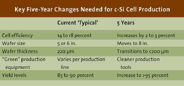
Continued worldwide growth in solar power as a renewable energy type is critically dependent on several factors: economic drivers (feed-in tariffs and subsidies), environmental changes (low carbon footprint production equipment), and technical enhancements (increased cell efficiencies and manufacturing yields). Although no formal road map has yet been approved, how the industry must change for it to continue to grow is beginning to be identified (see table). For several process steps, the implementation of these changes can be satisfied best through increased laser adoption.
Crystalline silicon cells
Crystalline-silicon (c-Si) and thin-film panels are the two distinct solar cell types in volume production today. Lasers can have the biggest impact in c-Si cell manufacturing because they hold a majority of the market — approximately 90 percent of all solar panels produced today and predicted to remain at 75 to 80 percent into 2015. In addition, there are a number of processes where lasers can be utilized within c-Si production. In contrast, thin-film solar manufacturing uses lasers primarily for just one process: thin-film patterning.1

Figure 1. This schematic represents edge isolation on c-Si solar cells, performed by laser scribing around the front surface. AR = antireflection.
Within c-Si solar panel production, fabrication is divided into two stages. Cells typically 125 or 156 mm wide and 220 μm thick are manufactured in a “back end” stage. The “front end” stage involves connecting approximately 60 to 70 cells in series to form a typical solar panel with a rated output power at the 200-W level. Laser processes find widespread use during the back-end stage.
Despite their advantages, lasers have not become overwhelmingly dominant in any of these steps. This is partially because many equipment vendors have offered entire turnkey production lines. Because of their backgrounds, these vendors have had a predisposition toward other process technologies; for example, plasma, wet-chemical etching equipment and screen printing. To spot opportunities, we must assess the advantages of laser-based systems compared with the alternative methods as they apply to the changes identified in the table.
Lasers offer greener processing
Greener processing is one of the clear advantages of lasers, particularly when compared with screen-printing/lithographic technologies. With solar energy purporting to offer a low carbon footprint solution to future energy requirements, it is not surprising that priority is given to production techniques with low environmental impact. Here, lasers, and in particular diode-pumped solid-state lasers, have an inherent advantage over other technologies, such as etching solutions, which use toxic chemicals and produce hazardous waste. Additionally, the idea of “green” laser-based tools immediately resonates with solar company mission statements and marketing campaigns.
Figure 2. Relative penetration depths are shown of 355 and 1064 nm, in c-Si.
But perhaps the most important benefit comes from the move to thinner wafers. Today, the dominant cost within c-Si solar cell manufacturing is the silicon raw material used at the back-end stage. As a result, reducing wafer thickness below today’s industry standard of 220 μm produces significant cost savings. Additionally, process costs potentially can be reduced by moving to larger-area wafers. However, thinner, larger wafers are increasingly fragile and mechanically vulnerable, so any form of contact processing can produce lower yields. Yet solar industry actually requires increased yields. Needless to say, the noncontact nature of laser processes offers profound benefits versus any contact-based alternative.
Edge isolation
The solar cell industry is being driven increasingly toward the use of lasers, supported simultaneously by equipment manufacturers producing tools specifically optimized for these applications. As an example of how this all comes together, the most widely used laser process in volume production for c-Si cell manufacturing is a technique known as “edge isolation.” This application exemplifies the issues at play because lasers compete with both plasma and wet-chemical etching solutions. It also shows how the characteristics of the laser sources evolved as both cell and laser manufacturers gained a better understanding of the process.

Figure 3. A 355-nm Q-switched diode-pumped solid-state laser produced an ∼20-μm-wide, ∼15-μm-deep groove in a c-Si solar cell.
Edge isolation is an essential part of all c-Si production lines, during which the front and rear surfaces of the silicon cell are electrically isolated after a phosphorus diffusion process that dopes the p-type silicon with an n-type top layer (Figure 1). Lasers scribe an isolation groove, typically 10 to 20 μm deep, to eliminate shunt pathways between the front and rear surfaces. The groove must be as close as possible to the edges of the front surface. Today lasers compete with both plasma and wet-chemical etching technologies, with the landscape split fairly evenly among them.2 In particular, wet-etching processes retain significant momentum within the solar industry because they are commonly used for saw damage removal after wafer dicing and for front-surface texturing. This places a higher emphasis on selecting the optimum laser source and process for any laser-based tooling to differentiate itself at the edge-isolation stage.
Laser optimization
Early laser-based tools suffered from problems typical of new capital equipment introduced into a high-volume production environment because they relied on the available 1064-nm wavelength. Current systems rely more heavily on diode-pumped solid-state lasers operating at 532 or 355 nm because of the significantly higher absorption of c-Si at these shorter wavelengths (Figure 2).3 Silicon absorption is four to five orders of magnitude stronger at 355 nm, compared with 1064 nm, allowing highly localized front-surface scribing when using Q-switched UV diode-pumped solid-state lasers. Besides shorter penetration depths, UV wavelengths allow narrower grooves to be scribed, minimizing the “dead” area around the edges and, consequently, maximizing the efficiency of the cell (Figure 3).
Another major motivation for cell manufacturers to switch to shorter wavelengths is to minimize subsurface “microcracks” that can be formed during 1064-nm processing. Microcracks are a key limiting factor because they decrease the yield of production lines. Any microcrack can result in cell failure during remaining back- and front-end production stages, at the panel installation phase or even because of stress from weather conditions such as heavy rainfalls or high winds. Reducing microcracks can be readily achieved by reducing the heat-affected zone through the use of 355-nm lasers.
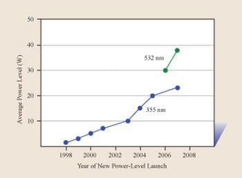
Figure 4. Shown are power level increases from industrial turnkey 532- and 355-nm AVIA Q-switched diode-pumped solid-state lasers.
An additional industry driver has been production throughput. Single-line production capacity has increased from 15 to 20 MW to more than 30 MW of annual cell output, while power scaling of industrial, end-pumped, Q-switched 532- and 355-nm diode-pumped solid-state lasers has kept pace (Figure 4). Power scaling to tens of watts of average power with beam quality M2 <1.3, combined with UV processing speeds >600 mm/s, represents the state of the art in laser edge isolation. This makes laser-based tools uniquely positioned to offer technical advantages over competing technologies, processing more than 3000 wafers per hour. As such, they are fully aligned to meet the needs of the industry over the next five to 10 years.
As other laser processes within c-Si manufacturing move from R&D or pilot phase to volume production, analogous issues to those encountered with edge isolation undoubtedly will occur. The availability of a diverse diode-pumped solid-state laser product portfolio that includes IR, green and UV outputs as well as nano- and picosecond pulse-width operation, will ensure that laser-based tools deliver the optimum solution and that the solar industry continues to grow.
Meet the authors
Finlay Colville is director of solar marketing and Corey Dunsky is senior manager of strategic applications, both at Coherent Inc. in Santa Clara, Calif.; e-mail: [email protected].
References
1. C. Dunsky and F. Colville (Feb. 14, 2008). Solid state laser applications in photovoltaic manufacturing. PROC SPIE, Vol. 6871.
2. O. Papathanasiou (Dec. 12, 2007). Wafer etching facts and trends. PHOTON INTERNATIONAL, pp. 128-139.
3. T. Gebel et al (October 2006). Millisecond annealing with flashlamps: Tools and process challenges, 14th IEEE Conference on Advanced Thermal Processing of Semiconductors.