Combining resonant microwave technology with atomic force microscopy allows measurement of slight variations of capacitance, dopant density, charge distribution and dielectric properties -- limited only by the sharpness of the probe.
Wenhai Han, Agilent Technologies Inc.
Mapping physical properties of various materials at high resolution has been pursued for decades in the microscopy world, and new challenges are added by the semiconductor and materials industries, which have an increasing need to map physical properties. The development of scanning tunneling microscopy in 1982 and of atomic force microscopy (AFM) in 1986 has significantly changed the world of microscopy. A number of methods derived from these techniques have been developed to probe the physical properties of materials.
For semiconductors, monitoring and controlling dopant levels — which correlate to changes of capacitance versus a change of voltage applied — in two and three dimensions play significant roles in the design process. Some ferroelectric materials with large dielectric constants are suitable for dielectric layers of microelectronic devices. Characterization of those materials at high resolution in two dimensions can provide better knowledge and understanding about their properties.
AFM-based scanning capacitance microscopy is capable of two-dimensional dopant profiling. Commonly used scanning capacitance microscopy uses an RCA capacitance sensor operating at 915 MHz and detects the capacitance-induced frequency shift. This technique, however, is widely used in a qualitative manner because of the lack of quantification processes. Capacitance mapping is highly limited because the stray capacitance is overwhelmed.
Scanning near-field microwave microscopy offers an alternative to mapping a material’s capacitance or dielectric properties. When based on scanning tunneling microscopy or on AFM, the method uses a metal or metal-coated probe in-line with a coaxial resonator. Capacitance is measured by detecting the frequency shift of the resonator. The resonator’s sensitivity for impedance mapping, however, is very restricted by the small signal-to-background ratio.
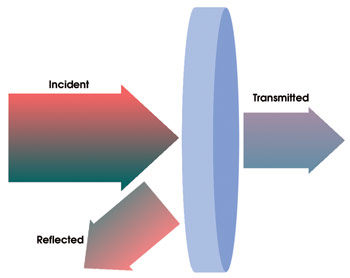
Figure 1. An optical analogy to microwave device characterization shows that some light is reflected while some passes through.
Network analysis has been widely used in microwave communications to characterize electrical properties of a device under test. To use optics as an analogy: When light strikes an object, some light is reflected, and some passes through (Figure 1). Measuring the amount of light reflected and/or transmitted reveals the optical properties of the object. The same principle can be used for the low-frequency microwave range (typically several gigahertz). For this, measurements of incident and reflected waves — and/or transmitted ones — can provide detailed information about the device being tested.
The most convenient instrument currently available to characterize a device using microwave waves is a vector network analyzer, or a professional network analyzer, which is a vector network analyzer with advanced features. Unlike a spectrum analyzer or a scalar network analyzer, a vector network analyzer can perform ratioed measurements (including phase), which provide a wealth of information about the device under test. For example, the information can reveal S-parameters, including complex coefficients for reflection and transmission as well as impedance.
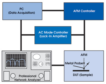
Figure 2. The scanning impedance probe microscope is based on the concept of integrating microwave network analysis technology into an AFM, which allows it to characterize properties at the resolution of an AFM. DUT = device under test.
Integrating microwave network analysis technology into an atomic force microscope provides a potential way to characterize physical properties of a device under test comprehensively and with the resolution of atomic force microscopy. The new scanning impedance probe microscope is based on that idea (Figure 2). The microwave is emitted from an internal source of the professional network analyzer and is transmitted through the microscope to the device under test (sample), where a conductive AFM probe makes contact. The probe also serves as a receiver to capture the reflected microwave from the sample and to feed it back into the network analyzer.
In the reflection mode (S11 measurement), the network analyzer measures the complex reflection coefficient G of the wave from the contact point. From the transmission line theory, G can be written as
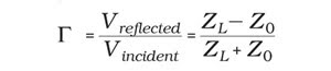
where Vincident and Vreflected are the incident and reflected waves, respectively, and where ZL and Z0 are, respectively, the impedance of the device under test and the characteristic impedance of the transmission.
The maximum sensitivity of Γ is obtained at the resonance where the impedance of the device under test matches the characteristic impedance. Near the resonance, the measured complex reflection coefficient corresponds directly to the impedance of the sample at the contact point. Small changes in the slightly mismatched impedance signal can be separated from the large background, resulting in a very high sensitivity. When the resistance variation becomes negligible, the measured impedance signal correlates to changes of the capacitance of the device under an appropriate phase lag. After calibration, the capacitance or dielectric properties of the sample are mapped simultaneously with the surface topography.
In traditional scanning capacitance microscopy, dopant profiling is performed by adding an alternating current (AC) bias to the sample and then measuring the resulting capacitance changes at a fixed AC bias, or by measuring the required AC bias that induces the same amount of capacitance variation. In the scanning impedance probe microscope, changes of capacitance from the reflected microwave as a result of a superimposed low-frequency modulation on the depleted carriers under the probe are detected by an AC mode controller containing a digital lock-in amplifier. Individual X- and Y-components as well as the total amplitude are measured to obtain both dopant type and density at the location where the tip contacts.
Besides physical properties of semiconductors and dielectric materials, the new scanning impedance probe microscope also may be used on organic films, polymers and even biological samples to measure a variety of properties associated with slight changes in impedance, both static and dynamic.
Those properties can be under the surface not observable from the topography image. By using a sharpened metal probe with a radius of curvature ∼10 nm, they can be mapped ultimately at a resolution down to several nanometers.
Meet the author
Wenhai Han is a senior scientist in the Nanotechnology Measurements Div. of Agilent Technologies Inc. in Chandler, Ariz.; e-mail: [email protected].