Novel materials and fabrication methods increase quality and lower cost of sensors for machine vision and industrial imaging.
Dr. P.K. Swain and David Cheskis, Sarnoff Corp.
Demand for higher throughput inspection systems with improved resolution is growing in the machine vision and industrial imaging industries. Traditionally, front-illuminated CCD or CMOS sensors are used in these inspection systems because of the lower costs associated with their high-volume manufacturing compatibility. To keep up with the increased demand, while remaining sensitive to cost constraints, manufacturers are forced to reduce the pixel size — limiting the performance of image sensors.
To solve this problem, sensor manufacturers are turning to back illumination. Back-illuminated image sensors are becoming more commonplace in high-performance imaging systems, given the inherent benefits when compared with their front-illuminated counterparts. However, their increased manufacturing complexity and high costs have constrained them for use in higher-end systems in the machine vision, semiconductor inspection and security markets. This has limited back illumination to a select number of products that are manufactured in low volumes at a few specialty foundries.
Recently, a breakthrough in novel materials and fabrication methods was achieved that will make higher-performance back-thinned imagers readily available for mass production. Using ultrathin silicon-on-insulator wafer technology, the method will reduce the manufacturing complexity and effectively solve the cost-quality challenge.
Back-illuminated image sensors
Fabrication of back-illuminated image sensors begins by using a standard front-side CCD or CMOS process. Once the process is completed, the substrate is thinned to form an optimized light-absorption region with additional color filter layers, antireflection coatings or micro-lenses applied to the back side of the wafer. A key step in achieving back-illuminated images involves thinning the silicon substrate in the range of 5 to 10 μm (sometimes even thinner) with a uniform thickness. It is challenging to attain such uniformity over the entire wafer, and it often results in lower manufacturing yield. Given that the wafer-thinning operation is performed as the last step, any yield loss significantly affects cost.
Starting with a carefully engineered silicon-on-insulator substrate, the buried oxide layer is used as a natural etch-stop to allow the ultrathin silicon to be used as a precisely controlled light collection region. This approach simplifies manufacturing significantly, improves uniformity and substantially reduces cost. Also, it allows easier scalability for wafers up to 300 mm in diameter. Choosing the proper buried oxide thickness can provide the desired antireflection coating. Use of a silicon-on-insulator substrate allows room for innovative designs as well, which can offer many other benefits, including lower power and better parasitics (Figure 1).
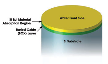
Figure 1. A cross section of an ultrathin silicon-on-insulator wafer used in imaging applications is shown.
System improvements
The increased fill factor of back-illuminated sensors can improve camera performance and lower cost in several ways. For applications requiring more resolution, one can shrink the pixel size to fit the existing chip area (Figure 2). On the other hand, die size can be reduced by up to 45 percent for a 4-megapixel sensor simply by using back illumination (Figure 3).
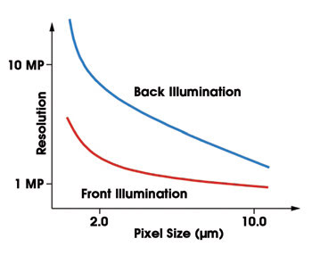
Figure 2. Resolution improves dramatically at smaller pixel sizes for a constant sensor size.
These advantages are important as the semiconductor industry continues to shrink the technology nodes and as the need grows for effective defect inspection tools (both wafer and photomask). To resolve submicron defects unambiguously, these cameras must be sensitive down to the deep-UV spectral region. The tools also must offer very high throughput to keep up with the ever-demanding price pressure of this industry.
Optimized back-illuminated sensors can extend the spectral range down to deep-UV levels while maintaining high and stable responsivity. They also improve the system’s performance by capturing more light, which improves the signal-to-noise ratio, increases the inspection speed and minimizes damaging UV exposure to delicate semiconductor devices.
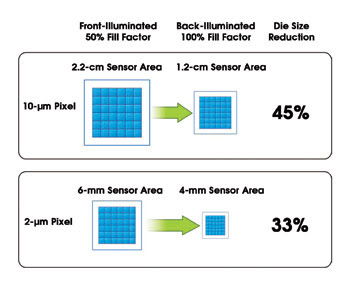
Figure 3. Reducing the die size of a 4-megapixel image sensor chip using back illumination leads to significant cost savings.
Machine vision and security systems require improved sensor performance for better resolution as well, and back-illuminated sensors benefit the total system cost by squeezing more performance from the existing optics. In systems where the optical components can add up to 25 percent of the total system cost, improving the image sensor performance can reduce such expense. This is achieved by improving the quantum efficiency of existing camera designs that have been reconfigured using back-illuminated sensors.
Using the ultrathin silicon-on-insulator materials for back-illuminated image sensors also provides compatibility with color filters and microlenses. This can enhance system performance in advanced applications such as food inspection and quality control.
Revolutionizing systems
Back illumination improves system performance in several areas, including better resolution, faster speed, more light capture, better signal-to-noise ratio, smaller die size and lower total imager cost. The key is that back illumination allows for a 100 percent fill factor by avoiding front-side features — transistors, metal routing — that reduce the amount of light available to reach each pixel.
Image sensors used in advanced inspection systems are revolutionized by improvements in back-illuminated technologies. New silicon-on-insulator materials are shattering the notion that back-illuminated sensors are too expensive, while new fabrication processes are bringing these sensors to the forefront of the imaging world. This innovative process will usher in an era of higher-performance inspection systems with lower costs and new features that will enable production of the ever-smaller semiconductors required by the industry.
Meet the authors
P.K. Swain is director of engineering and David Cheskis is business director, both with the Imaging Systems group at Sarnoff Corp. in Princeton, N.J.; e-mail: [email protected]; [email protected].