
TEAM Yields Stunning Images
The world's most powerful transmission electron microscope has been used to produce stunning images of individual carbon atoms in graphene, the two-dimensional crystalline form of carbon that is highly prized by the electronics industry.
Using TEAM 0.5 (transmission electron aberration-corrected microscope), researchers with Lawrence Berkeley National Laboratory (Berkeley Lab) recorded the images for the first time at Berkeley Lab's National Center for Electron Microscopy (NCEM). TEAM 0.5, its newest instrument, is capable of producing images with half-angstrom resolution, which is less than the diameter of a single hydrogen atom.
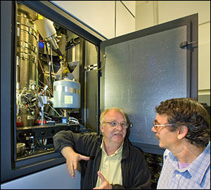
Christian Kisielowski (left) and Alex Zettl, scientists with the Lawrence Berkeley National Laboratory, at the TEAM 0.5 microscope, which enables scientists to see each and every individual atom in a sample, a huge advantage for scientists who study materials and their properties. (Images: Berkeley Lab)
“Simply put, TEAM 0.5 is the best transmission electron microscope in the world, representing a quantum leap forward in instrumentation,” said physicist Alex Zettl, who led the research. “Having the ability to see, basically in real time, each and every individual atom in a sample is unbelievably useful and the images we can now see have been jaw-dropping for even the most seasoned electron microscopists. TEAM 0.5 is pushing transmission electron microscopy to a new level.”
The properties of solid materials stem from the arrangement of their constituent atoms in the solid’s crystal structure. While technologies such as electron and x-ray crystallography can reveal the atomic geometry of a crystal, they do not identify the precise location and position of each individual atom. When the dimensions of a material shrink to the nanoscale, the location and position of each individual atom becomes critically important, Zettl said.
“Think of the steel rebars on a three-dimensional structure, like a jungle gym,” he said. “If a small piece of rebar is rusted out somewhere in the center of the gym, it won’t likely have much affect on the overall properties of the structure. In a two-dimensional structure, however, a rusted out segment becomes a much bigger problem, and in a one-dimensional structure, i.e., a single rebar, a rusted out segment can be catastrophic, causing the entire structure to fail. On a nanoscale crystal, one missing atom or some other defect in the arrangement can result in catastrophic failure.”
Graphene is especially sensitive to defects in its atomic structure. Consisting of a single-layered sheet of carbon atoms arranged in hexagons, like a sheet of chicken wire with an atom at each nexus, graphene features extraordinary electrical, mechanical and thermal properties that could enable it to serve in a broad array of carbon-based electronic devices. For the enormous promises of graphene to be fulfilled, however, scientists need a much better understanding of how specific types of defects in the crystal structure, including those that change location over time, affect its properties.
“Theorists are currently making all kinds of predictions about the properties of graphene for different local atomic configurations, but until TEAM 0.5, we did not have the ability to actually see and study these configurations in real time,” Zettl said.
TEAM 0.5 features state-of-the-art technical advances including an extremely bright electron source, ultrastable electronics to reduce drift and, perhaps most importantly, the ability to provide optical corrections for spherical aberration (blurring). By making points of light look like disks, spherical aberrations have been the prime limiting factors in the resolution of transmission electron microscopy.
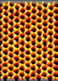
An image of a single suspended sheet of graphene taken with TEAM 0.5 shows individual carbon atoms (yellow) on the honeycomb lattice.
“TEAM 0.5 allows for the detection of every single atom from the Periodic Table provided that the sample under investigation can stand the radiation damage (TEAM 0.5’s record-setting half-angstrom resolution was achieved with an electron beam that was 300 kilovolts (kV) in energy.)," said Christian Kisielowski of NCEM, who collaborated on the research.
Correcting spherical aberration makes it possible to use the TEAM 0.5 not only for broad-beam “wide-angle” images but also for scanning transmission electron microscopy (STEM), in which the tightly focused electron beam is moved across a sample as a probe.
In this mode, TEAM 0.5 is capable of performing spectroscopy on one atom at a time — an ideal way to precisely locate impurities in an otherwise homogeneous sample, such as individual dopant atoms in a semiconductor. Aberration correction also enables TEAM 0.5 to produce high resolution images at relatively low electron beam energies. Because of their longer wavelengths, lower energy electrons are more difficult to focus than higher energy electrons. Aberration correction overcomes this problem.
Using TEAM 0.5, Zettl, Kisielowski and their collaborators were able to obtain images of graphene membranes -- crystalline foils 1-atom thick -- at a resolution of one angstrom using electron beams of a mere 80 kilovolts (kV) in energy.
“The low voltage was crucial for the stability and study of these graphene membranes which are much too fragile to be imaged at the higher energies required for conventional transmission electron microscopy,” said Zettl. “That we were able to detect and resolve every individual carbon atom in these foils at 80 kV is relevant for future studies of organic materials where low-z atoms dominate and higher energies are damaging to samples. TEAM 0.5 provides fantastic resolution at low electron energies, which is the best of both worlds for organics.”
“This is not even the end of the story. We have since made improvements to further boost signal-to-noise ratios and already have new and even better images. There is much more to come,” added Kisielowski.
TEAM 0.5 was designed and constructed through a collaboration led by Berkeley Lab and including Argonne and Oak Ridge national laboratories, the Frederick Seitz Materials Laboratory of the University of Illinois, and two private companies specializing in electron microscopy, the FEI Co. of Portland, Ore., and CEOS of Heidelberg, Germany.
Zettl holds joint appointments with Berkeley Lab’s Materials Sciences Div. (MSD) and the Physics Department at the University of California’s Berkeley campus, where he is the director of the Center of Integrated Nanomechanical Systems. Collaborating with him and Kisielowski on the project were Jannik Meyer, also with Berkeley Lab’s Materials Sciences Div., and Rolf Erni and Marta Rossell of NCEM.
Their results were published in the journal Nanoletters, in a paper entitled: “Direct Imaging of Lattice Atoms and Topological Defects in Graphene Membranes.”
For more information, visit: www.lbl.gov
Published: September 2008