Determining the Right Method for the Job
Robert J. Crase, Deposition Sciences Inc., and Dr. Margareta Hamel, Auer Lighting GmbH
Chances are that this magazine comes off a press that uses components with thin-film coatings. What’s more, your supermarket checkout scanners, cell phones, cars and TVs all utilize thin-film coatings. Despite the wide range of applications, there are just five basic deposition methods for manufacturing thin films, and the designer needs to know them well. They are:
Electron beam evaporation (ebeam); low pressure chemical vapor deposition (LPCVD); plasma impulse chemical vapor deposition (PICVD); magnetron sputtering; and ion beam sputtering (IBS). Knowing the strengths and weaknesses of each is essential.
1. Electron Beam technology, the most widely used, has the source material placed into a “pocket” in an electron beam gun (Figure 1). The gun produces a stream of electrons that are steered by a series of electromagnets onto the coating material. When the beam heats the material, it evaporates and moves toward the top of the chamber, where it is deposited onto the substrates. To improve uniformity, the substrates are rotated around the chamber in either a single or double rotation system. To improve durability, the chamber is heated to a nominal 300 °C, and an ion beam gun is added, which is directed at the substrates to increase coating density. The thickness of individual layers is controlled via an optical monitor.
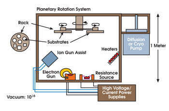
Advantages: Ebeam systems are versatile and can be reconfigured quickly from one coating type to another simply by changing source materials. Employing an optical monitor allows production of precise coatings. The systems use relatively small amounts of material for each run, making the cost of entry for a single coating quite low – a consideration when depositing precious metals such as gold, platinum and rhodium.
Disadvantages: Because ebeam systems use the top of the chamber as the deposition location, they are limited to a circular load size. This can be increased with a larger coating chamber, but large-area chambers have difficulty producing precision filters. The deposition speed of an ebeam chamber is relatively slow compared with some other technologies, and the chamber temperature is high, making it difficult to coat some glass types and plastics. Ebeam coatings also tend to be less dense, making them less durable than other technologies. Because it is a line-of-sight technology, it is difficult to uniformly coat shaped optics.
2. Low Pressure Chemical Vapor Deposition is commonly used in the semiconductor industry (Figure 2). Deposition Sciences Inc. of Santa Rosa, Calif., and others have adapted the technology to deposit optical thin films. LPCVD is a thermally driven chemical reaction process in which the starting materials are metallorganic liquids called precursors. These are delivered to an evaporation manifold and vaporized. Then a flow of nitrogen gas carries the vapor into the reaction chamber. The chamber is held at a nominal 500 °C. The heat breaks the chemical bonds in the precursors, and the resultant metal oxides condense onto the surfaces in the chamber. The waste products and unreacted material are swept out of the system by a nitrogen flow to a condenser manifold, which is held at cryogenic temperatures, causing the waste products to become trapped. The nitrogen is then pumped out.
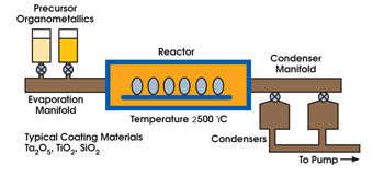 Advantages: The LPCVD process coats uniformly, which makes it possible to coat optics with complex shapes. This is well suited for domes and reflectors with very high aspect ratios (reflector opening to reflector depth). Domes as large as 190 mm and reflectors with aspect ratios as high as 4:1 have been coated successfully in the LPCVD system at Deposition Sciences. LPCVD coatings are very dense, making them mechanically, thermally and environmentally durable. They also exhibit very little wet-to-dry shift with changes in temperature and humidity.
Disadvantages: LPCVD is thermally driven and takes place near 500 °C, so substrates must remain stable at those temperatures. Plastics and glasses with low melting points cannot be coated in these systems. The process is relatively slow compared with other methods; e.g., a visible antireflection coating takes four hours to coat, compared with less than one hour in a sputtering system. In thick films, a high degree of residual stress can build up, causing the film to self-destruct. The choice of precursors – and therefore coating materials – is limited. A typical coating process is limited to wavelengths from 350 to 2500 nm.
3. Magnetron Sputtering is used in the architectural window glass coating process, with in-line systems that coat hundreds of square feet per minute (Figure 3). It also is used to deposit precision thin films. In a magnetron sputter system, there are cathode assemblies containing magnets. The face of these cathodes has a plate of coating material called a target. After the coating chamber is evacuated, it is backfilled with a working gas, typically argon. A voltage is applied to the cathode assembly. The electrons are contained in front of the cathode by the magnetic field. As electrons hit the argon atoms, the electrons are knocked off the argon atoms, causing them to become positively charged. A plasma of ionized argon forms in front of the target. The positively charged argon ions are accelerated toward the negatively charged target, where they strike the face of the target-ejecting metal atoms. During this process, a reactive gas, typically oxygen or nitrogen, is introduced. To ionize the gas, Deposition Sciences employs its MicroDyn system using a microwave source. The gas combines with the metal atoms from the target to form the desired metal oxide or nitride. Typically, the material sources, or targets, are around the periphery of the chamber, and the substrates are held on the surface of the drum in the center. The drum rotates so all parts are coated.
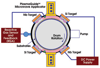 Advantages: By loading substrates onto the surface of a cylinder load sizes can be large, and deposition rates high. A visible antireflection coating can be deposited in less than an hour. Magnetron sputtered films are dense, making them mechanically, environmentally and thermally durable with thin films that can operate at temperatures of up to 1000 °C. This density allows them to avoid wet-to-dry shift. Stress in the films can be modified and controlled for different materials, which enables production of thin films that are nearly stress-free. Independently controlled target plates provide a different uniformity profile for each material. Two materials of different indexes can be co-sputtered to form a material of an intermediate index. This index can be varied over a wide range. Because the process is low-temperature, plastics and other materials with low melting points can be used.
Disadvantages: The process occurs at a relatively high pressure – several torr – causing the films to have a higher scatter component than other methods. This can make the films less than ideal for applications such as deep-UV coatings, high-power laser coatings and ultrahigh reflectors, R >99.9 percent. Material costs can run high because it is necessary to purchase large amounts of material to form the target, as opposed to using only a few grams of a material for the ebeam system. Magnetron sputter systems also take longer than ebeam systems to change over between jobs.
4. Ion Beam Sputtering is similar to magnetron sputter systems; i.e., both systems use a target of coating material and a stream of ions to sputter material from the target (Figure 4). This is where the similarity ends. In an IBS system, the ion gun directs a stream of ions at the target at a 45° angle, causing metal atoms to be knocked off. The sputtered material then deposits onto the substrates, which are rotated in either a single or double rotation system. Film thickness is controlled through a monitor system. In IBS, the working gas and the reactive gas are combined in the ion gun so metal atoms are sputtered and oxidized simultaneously.
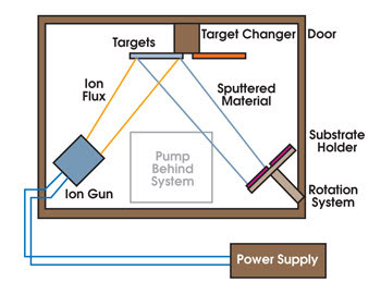 Advantages: IBS can produce some of the lowest-loss thin films. Typical absorption and scatter losses are measured in low parts per million. This low scatter and absorption make them well suited for high-power laser, ultrahigh-reflectance coating, R >99.99 percent and deep-UV applications. The system monitor allows IBS to produce extremely precise, ultradense and durable coatings with no wet-to-dry shift.
Disadvantages: IBS systems have a very slow deposition rate. An antireflection coating in the visible takes many hours, making it less than ideal for high-volume production. The load and maximum sizes of a substrate that can be coated are small. Typical systems can coat substrates up to several inches in diameter. IBS coatings have very high residual stress. A relatively thick, high reflector deposited onto a thin substrate causes a substrate to deform. IBS, as with ebeam, is a line-of-sight deposition technology, making it difficult to coat shaped optics uniformly.
5. Plasma Impulse Chemical Vapor Deposition is a combination of CVD and microwave plasma (Figure 5). The coating chamber is the reflector to be coated, which is filled with gaseous precursors similar to the LPCVD process. When the chamber is filled completely, a microwave pulse ignites a plasma. The plasma decomposes the precursor in the coating materials, either SiO2 or TiO2, depending on the precursor. The reaction products condense on the surface of the reflector, and the process is repeated with a new precursor.
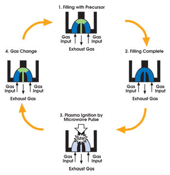 Advantages: The process is highly stable, and the layer thickness can be maintained accurately by controlling gas flow and the number of microwave pulses. Control of the pulses guarantees a precise input of energy in the deposition process. The coating temperatures can be varied widely for coating glass (high) or polymers (low). The PICVD process has a deposition rate of several hundred nanometers per minute for oxides. The total deposition time for a visible cold mirror is a few minutes. PICVD coatings are very dense, with no wet-to-dry shift. They are extremely mechanically, environmentally and thermally durable, with thin films that can operate at temperatures up to 450 °C.
PICVD is well suited for coating the inner and outer surfaces of three-dimensional structures. Cold mirrors can be fabricated on reflectors from 35 to 230 mm in diameter. PICVD also can be used to coat the outside surface of substrates.
For these, a chamber is lowered over the part to be coated. This process is used extensively in the deposition of a hot mirror or infrared coating on halogen lamp burners. This highly efficient halogen (HEH) lamp can save 30 percent energy. The process is automated easily and can produce millions of parts per year.
Disadvantages: The process uses a microwave pulse to cause the precursors to react. Substrates coated in the PICVD system must be compatible with microwaves, making it difficult to coat metal or ceramic substrates. The process coats one part at a time, requiring many stations for high volume production. As in the LPCVD process, the coating materials are limited by the availability of precursors. This limits the wavelength range over which coatings can operate from 350 to 2500 nm.
The use of thin films is growing daily, and coating facilities worldwide offer an abundance of deposition technologies. It is important for the engineer, buyer, designer and user to understand that all deposition technologies are not equal. Each is unique and better suited for certain applications than others. Understanding this is the key to an optical system that is designed to last and that will perform as designed.
Meet the Authors
Robert J. Crase is program manager for manufacturing operations at Deposition Sciences Inc. in Santa Rosa, Calif.; e-mail:[email protected] .
Margareta Hamel is manager of research and development for thin-film technology at Auer Lighting GmbH in Bad Gandersheim, Germany; e-mail: [email protected].
Both companies are part of the Advanced Materials Group of Advanced Lighting Technologies Inc. of Solon, Ohio.