Imperfections in solar cells often can’t be seen with the naked eye, but they can cause real problems when the cell is installed in a photovoltaic module. Inconsistencies or failures jeopardize manufacturer warranties and greatly limit energy production. Vision system and camera vendors are lining up to join the solar market.
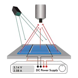
A schematic of a setup for camera-based solar cell inspection is shown under operating conditions. Courtesy of the Institute for Solar Energy Research.
Photovoltaic solar cells are generally either crystalline silicon or thin film. The main difference is that wafer inspection is not necessary with thin film because its production process yields modules rather than cells. Nevertheless, vision systems are used to inspect the geometric properties, contour integrity and tiny cracks in both types.
Silicon CCD cameras are used in imaging solutions offered by Andor Technology plc of Belfast, UK. Coming from the scientific imaging community, electron-multiplying CCD cameras provide very low readout noise and high near-infrared sensitivity, providing the basis for vision systems suitable for solar cell in-line inspection.
Meeting the demand
Using electroluminescence (EL) and photoluminescence (PL) imaging, Andor’s Luca-R electron-multiplying CCD camera can determine to what extent efficiency may be compromised by defects in thin electrodes printed on top of the cell or by microcracks. The camera offers high sensitivity, low noise and resolution of 1 megapixel at high frame rates as demanded by in-line inspection systems running at speeds of one cell per second and faster.
According to Karsten Bothe, head of the Solar Cell Characterization Group at the Institute for Solar Energy Research in Emmerthal, Germany, defect-related luminescence is not detected within the 900- to 100-nm wavelength. It is the band-to-band luminescence caused by radiative recombination of carriers that is detected. This emission is high if there are no defects and decreases with increasing defect density. Defect-related luminescence is visible only at lower energies and, thus, at larger wavelengths around 1500 nm. That’s one of the benefits of InGaAs cameras, he noted.
Bothe’s group tests EL and PL imaging solutions at the institute, and he believes that both types of imaging will be “very powerful characterization tool(s) in the near future.” He said any black-and-white camera is capable of both types of imaging, adding that such cameras are produced by traditional manufacturers, including the German-based PCO AG and Sensovation AG, the Japan-based Hamamatsu and others.
Coming from the machine vision world, Dalsa Corp. of Waterloo, Ontario, Canada, recently announced its entry into this market. Using time-delay integration technology with a CMOS sensor, its solution can capture images at 62 fps with 4-megapixel resolution. Bothe pointed out that CMOS usually has shorter readout times of the sensor.
How to choose?
“For me as a user, I don’t care which camera technology is used,” Bothe noted, adding that InGaAs is another appealing option, although much more expensive and the resolution currently lower.