Solar manufacturers
have a few technologies at their disposal that can detect cracks in cells and modules.
In an industry where energy efficiency is the name of the game, manufacturers want
to reduce or eliminate cracks to improve yield, reduce waste and avoid putting faulty
modules into solar panels. Defects are detected with various types of imaging (see
“Camera makers find a niche in the solar market,” page 43, May 2009),
but some companies prefer to begin with resonance ultrasonic vibration (RUV) technology.
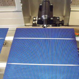
Resonance ultrasonic vibration is used to inspect solar cells on the assembly line. Photo courtesy of RUV Systems.
The process known as RUV was invented and developed by Dr. Sergei
Ostapenko, who conducted his research at the University of South Florida in Tampa.
Initially, his projects focused on measuring stress in silicon wafers for microelectronics.
But with a personal interest in photovoltaics (PVs) and an involvement in numerous
PV projects at the university, his research moved quickly in that direction.
His team found that resonance vibration modes in wafers could
be measured while they were running along the production line. The group also developed
data analysis software; both technologies became the basis for the launch of Ultrasonic
Technologies Inc., a startup based in Tampa, Fla.
The way it works, according to Ostapenko, is basically akin to
tapping on several identical new wine glasses. A glass with a crack in it will sound
different from an undamaged one. “Ultrasonic testing does the same thing with
silicon wafers and solar cells, but at a frequency range above what you can hear
with your ear, which ultimately increases crack detection sensitivity and accuracy,”
Ostapenko explained. On the production line, RUV also allows fast real-time crack
inspection, matching throughput of solar cell wafers and modules at a few seconds
per unit.
Optical testing an option
Yield and quality are directly related to finding and rejecting
unstable wafers or cells while they are still on the assembly line, manufacturers
find. This can be achieved with RUV, so the technique can eliminate the need for
optical testing. However, if discarding defective units is not the sole goal and
locating the crack is essential, optical testing off-line can perform this function.
The main difference between RUV and optical methods is that RUV
is “listening” to the cracks rather than seeing them. Manufacturers
can use both techniques first by listening to the cells and then, as a backup, using
infrared or electroluminescent (EL) inspection on any wafers or cells that are rejected
or questionable.
A clear strength of optical testing, said Ostapenko, is its ability
to get a visualization of the full wafer. However, the drawbacks of using optical
testing alone include its inability to see tiny, sealed cracks, or to distinguish
between a surface scratch and a true crack. Furthermore, he added, EL imaging can
be applied only to finished cells and cannot be used on wafers, which don’t
yet have electrical contacts to which the bias voltage needed for EL would be applied.
Similarly, infrared transmission imaging can be used exclusively on bare wafers
and cannot be applied to processed material with a nontransparent back contact.
The RUV method, on the other hand, is applicable to the entire silicon cell production
process, from wafers to finished cells.
When RUV is used in conjunction with optical inspection, the two
technologies complement and reinforce one another. Rimas Systems BV is a Dutch manufacturer
of solar module manufacturing equipment. At RUV Systems, a company partially owned
by Rimas, RUV technology is being implemented in inline production equipment for
module, cell and wafer manufacturing. RUV Systems, in cooperation with Ostapenko,
also studies RUV in conjunction with optical imaging.
According to Michel van Dooren, plant manager at RUV Systems,
RUV technology is “the most reliable for detecting cracks in an in-line situation.”
He added that optical imaging is best for analyzing the rejects off-line, where
there is more time to make the image. Using the two technologies in conjunction
helps to reject faulty product from the assembly line and then validate the problem
with an image.