Marcus Wallace and Henry Orr, NDC Infrared Engineering Ltd.
Near-infrared filters operate within a wavelength range of 800 to
5000 nm and typically consist of multiple thin-film interference layers of silicon/
silicon compounds deposited on a suitable optical substrate. They can be manufactured
in narrow- and wideband filters and in cut-on/-off varieties, and they have applications
in both terrestrial-based IR telescopes and in satellite IR measurement payloads.
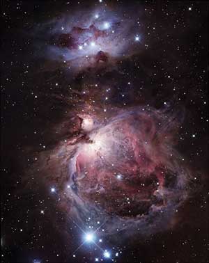
Orion Nebula as
captured by VISTA in visible light. Image by ESO; J. Emerson, VISTA; and R. Gendler.
Courtesy of Cambridge Astronomical Survey Unit.
Filter manufacturing techniques
Near-IR filters generally are produced using vacuum deposition
techniques. The choice of the technique determines the structure of the thin films
being deposited.
Traditional vacuum deposition methods involve thermal evaporation
of the bulk material, with electron beam excitation being the most popular. The
optical material is heated in vacuum until it sublimes or becomes molten, to produce
a dispersed vapor within the vacuum process chamber. Each layer is built up progressively,
as the vapor condenses uniformly across the surface of the prepared optical filter
substrate.
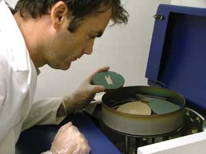
Figure 1. Pulsed-DC magnetron sputtering system. Images courtesy
of NDC Infrared Engineering Ltd.
An alternative method is pulsed-DC magnetron sputtering. One technique
uses a single-fixed-source sputter target of high-purity silicon and a high-power-pulsed-DC
power supply1 (Figure 1). By choosing different sputter gas combinations (argon,
nitrogen or oxygen), various filter layers can be produced. Key filter parameters,
indicated in Figure 2, are peak wavelength and transmission, bandwidth and blocking
region.
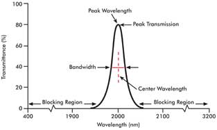
Figure 2. Near-infrared narrowband filter characteristics.
Bandwidth is controlled by the design of the filters and the material
properties. This is achieved by optimizing the manufacturing process to deliver
the same material properties repeatedly for each filter. Peak wavelength and bandwidth
are determined by selecting the appropriate number, composition and thickness of
filter layers deposited, and the substrate used. In this way, a wide range of filters
can be manufactured with peak wavelengths ranging from 400 to 5000 nm and bandwidths
from 1.0 to 14 percent full width half maximum.
Blocking filters are established by coating the back surface of
the filter substrate with another multilayer of dielectric wideband filters, which
typically have bandwidths upward of 14 percent.
Filters for IR telescopes
Instruments such as those on WFCAM2 (Wide-Field Camera on UK IR
Telescope on Mauna Kea in Hawaii) and VISTA3 (Visible & Infrared Survey Telescope
for Astronomy, European Southern Observatory in the Atacama Desert of Chile) require
filters operating from 0.8 to 2.4 μm. WFCAM is composed of four Hawaii-II 2048
x 2048 x 18-µm-pixel array detectors from Rockwell Scientific, with a pixel scale
of 0.4 in. (f/2.4) and a field of view per exposure of 0.21 square degrees.
Each detector is divided into quadrants, with each of those divided
into eight channels of 128 x 1024 pixels. The detectors are spaced at 94 percent
of the detector width. Four exposures are required to survey a contiguous area (tile)
of 0.8 square degrees. WFCAM has eight filter housings, including the broadband
set Z/Y/J/H/K, and two narrowband filters, H2 and Br-Gamma. The eighth filter housing
is blanked for darks. The Y, J, H, K, H2 1-0 S1 and Br-Gamma band filters are manufactured
by NDC Infrared Engineering Ltd. using the pulsed-DC magnetron sputtering technique.
The filters’ specified bandpasses are shown in Table 1.4
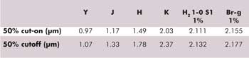
Table 1. Bandpasses of NDC Infrared Engineering filters for WFCAM.
A major challenge to producing narrowband filters in this region
of the spectrum using thermal evaporation techniques is loss of transmission efficiency,1
particularly noticeable for Si/SiO filters at wavelengths in the 1200- to 1300-nm
range. Typical transmission efficiencies at these wavelengths can be on the order
of 60 percent, compared with 70 to 80 percent at higher wavelengths.
For high-refractive-index semiconductor film materials such as
silicon and germanium, the packing density in films produced by thermal evaporation
is less than the bulk or crystalline form of the material. Films deposited in this
way can have a poorer definition of the absorption edge and are generally less transparent.
The reasons are associated with the fact that the substrate temperature is significantly
lower than that of the vapor, and there is insufficient energy in the vapor molecules
to anneal the film structure into a dense solid similar to that of the bulk form
of the material.
Although things can be improved somewhat by raising the temperature
of the substrate, the pulsed-DC magnetron sputtering technique offers some significant
advantages. It produces a vapor with much higher energy, enabling films to be deposited
with well-ordered structures and near-bulk packing density, and, by choosing different
sputter gases, silicon-monoxide, silicon-dioxide and silicon-nitride films also
can be deposited, offering improved transmission at wavelengths down to 700 nm.
The benefits of this approach are illustrated in the case of the
1185-nm filters used on VISTA. At the heart of VISTA is a 3-ton camera containing
a 16-detector array. Figure 3 shows a comparison of in-band transmission for the
1185-nm filter produced using a sputtered Si/Si3N4 film stack process and a similar
filter produced using a conventional evaporated Si/SiO film process.
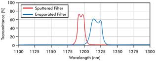
Figure 3. Comparison of in-band transmission for sputtered versus evaporated filters of similar wavelengths.
The sputtering process produces a filter with not only better
transmission but also a narrower bandwidth. Even more challenging was the requirement
by Oxford Astrophysics, a department of the University of Oxford in the UK, for
matched sets of filters to operate at 975 and 985 nm on VISTA.1 The center wavelength
of these filter sets falls within the spectral range most affected by silicon film
optical absorption, and the specification (Table 2) requires a narrow bandwidth
of approximately 1.1 percent of center wavelength.
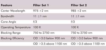
Table 2. Summary specifications by Oxford Astrophysics for 985- and 975-nm filter sets on VISTA.
To optimize transmission at these low wavelengths, the narrowband
“peak” coating was designed using a Si3N4/SiO2 multilayer structure,
which minimized the in-band optical losses. The blocker coating design was Si/Si3N4,
but with some modified gas parameters for the silicon layers, which introduced a
partial oxidation state. The result was excellent in-band transmission of ~80 percent
for the 975- and 985-nm bands.
Another significant benefit offered by the sputtering technique
is the reduced spectral shift exhibited by the sputtered filters under cryogenic
conditions.
Filters for satellite payloads
Besides the application to shorter wavelength filters shown above,
the pulsed-DC magnetron sputtering technique has been applied to filters for longer
IR wavelengths, encompassing the upper limits of the InSb detector spectrum. It
will be used on the INSAT-3D weather satellite, which is due for launch by 2011.5
The INSAT-3D instrument is an advanced infrared geostationary
meteorological satellite being developed by the Indian Space Research Organisation
Space Applications Centre for high-resolution monitoring of temperature and trace
chemical species in the regions between the troposphere and stratosphere.
The instrument comprises a six-channel imaging radiometer designed
to measure radiant and solar reflected energy from areas sampled on Earth, and a
high-resolution infrared sounder to measure vertical temperature profiles, humidity,
surface and cloud-top temperatures, and ozone distribution. Six short-wavelength
infrared filters for the sounder covering the wavelength center range of 3.75 to
4.57 nm were produced using the pulsed-DC magnetron sputtering technique.6
The reduced spectral shift with temperature for filters produced
in this way has contributed to the filters passing the environmental and spectral
aging stability requirements for the mission according to standard ESA-PSS-01-702.
Meet the authors
Marcus Wallace is optics supervisor and Henry Orr a consultant,
both at NDC Infrared Engineering Ltd. in Maldon, UK; e-mail: [email protected];
Email: [email protected].
References
1. H.J.B. Orr et al (2008). Near-infrared bandpass filters with
improved transparency for 1000nm spectral region using sputtered silicon compound
films. Proc. SPIE, Vol. 7018, pp. 701830-701830-12.
2. http://www.roe.ac.uk/atc/projects/wfcam
3. VISTA: http://www.eso.org/public/teles-instr/surveytelescopes/vista/camera.html
4. WFCAM instrument filters: http://www.ukidss.org/technical/technical.html
5. INSAT-3D:http://www.reading.ac.uk/infrared/research/projects/ir-isro.aspx
6. G.J. Hawkins et al (2008). High-performance infrared narrow-bandpass
filters for the Indian National Satellite System meteorological instrument (INSAT-3D).
Applied Optics, Vol. 47, No. 14.