Hank Hogan, Contributing Editor
Sometimes you don’t want 2 + 2 to equal 4. Instead, it would be nice if the result were
a lot more – or a lot less.
That’s the basis for nonlinear optical processing, where
a material or device has an outsize response to incoming light. With that, it is
possible to convert one frequency of light into another. Other outcomes can be optical
parametric amplification, supercontinuum generation or fast switching. Nonlinear
effects can lead to Raman lasers and other tools – including what could be
the foundation for tomorrow’s computers.
To get a sense of where nonlinear optical processing is headed,
a good place to look is the Optical Society of America (OSA)’s Nonlinear Photonics
Topical Meeting, held this year in late June in Karlsruhe, Germany. Karsten Rottwitt,
one of the program chairmen, reported 218 accepted papers, the largest number in
years, and many more submitted. “It was very successful in terms of numbers
of papers. I think that indicates a huge interest in the field.”
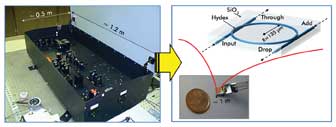
By exploiting nonlinear optical phenomena, researchers turned a tabletop
oscillator (right) into a photonic chip (left). Courtesy of Marcello Ferrera and
Dr. Luca Razzari, Ultrafast Optical Processing Group, INRS-EMT.
Rottwitt, an associate professor of photonics at Technical University
of Denmark in Lyngby, noted that, in the past, the focus had been on optical communications.
Today, applications in sensing and lasers are increasingly important, as are wavelengths
other than the 1500-nm telecom standard.
What has not changed is the focus on new materials and new devices.
Innovations in the first are particularly needed, Rottwitt said. An ideal material
would be one with high nonlinearity, low loss, little two-photon absorption and
easy processing.
On the device side, what is needed is compatibility with standard
electronics and a nonlinear response. An example of this can be found in an integrated
multiple wavelength laser source that was described in a paper at the OSA meeting.
The device has a total conversion efficiency of almost 10 percent and frequency
spacing of more than 6 THz from 1400 to 1700 nm, an important communication range.
It also has another important attribute.
“This material platform is the first CMOS-compatible platform
that has been shown to be capable of very high nonlinear optical performance,”
said research team member David J. Moss.
A physics professor at the University of Sydney in New South Wales,
Australia, he noted that silicon has attracted considerable interest for a good
part of the past decade as a nonlinear optical material. However, because it suffers
from two-photon absorption, researchers have been looking for alternatives compatible
with standard CMOS processing.
Moss, a group from the National Institute of Scientific Research
– Energy, Materials and Telecommunications (Institut National de la Recherche
Scientifique – Énergie, Matériaux et Télécommunication)
in Quebec, and two researchers from Annapolis, Md.-based Infinera Corp. devised
a solution based on a doped silica glass microring resonator. The ring measured
270 µm across and had a waveguide core about 1.5 μm square. To create that
core, they buried a low-loss, doped glass with a refractive index of 1.7 inside
standard silicon dioxide, which has a refractive index of 1.45.
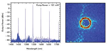
Shown is output from a miniature multiple wavelength source (left) based on a ring resonator and an InGaAs camera image of the ring resonator in resonance conditions (right). Courtesy of
Marcello Ferrera and Dr. Luca Razzari, Ultrafast Optical Processing Group, INRS-EMT.
The high-index glass is a proprietary blend, the rights to which
are owned by Infinera. However, Moss said that any material with the right properties
would do. What is needed, he said, are low linear and nonlinear loss, a high optical
nonlinearity and a high linear refractive index contrast, as compared with normal
optical fiber.
The proprietary formulation used by the researchers allows the
creation of a low-loss film without the need for high temperature annealing. That
is what makes the device and material CMOS-compatible.
The researchers measured the performance of their device, which
works on third-order nonlinearities. They found the full width half maximum of the
linear optical transmission spectrum to be 1.3 pm at 1544 nm, indicating a quality
factor of about 1.2 million.
Moss reported that a number of companies have expressed interest
in the device, which has possible application for next-generation telecommunications
or as a means to optically interconnect computers. He cautioned, however, that research
is ongoing as to what may be possible with such devices.
As for making devices such as this, it wouldn’t require
a breakthrough or exotic manufacturing, Moss said. “A fairly standard semiconductor
processing lab with cleanrooms and good lithography would suffice, so it is not
that unique.”
Besides new devices, nonlinear optical processing also would benefit
from new materials. In that regard, a nanowire design from researchers at Australian
National University in Canberra showed a huge nonlinearity. They reported that they
had achieved the highest nonlinearity ever obtained for a glass waveguide. What’s
more, their construct had negligible two-photon and free-carrier absorption, leading
to a nonlinear figure of merit 200 times that of silicon at 1550 nm.
They did this using chalcogenide glass, a mixture of germanium,
arsenic and selenium. Coming up with the right formulation was a challenge, said
research leader Barry Luther-Davies.
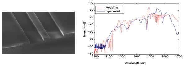
Nanowires (above) of chalcogenide glass generated the supercontinuum
spectrum (right). Courtesy of Barry Luther-Davies, Australian National University.
“The physical properties of chalcogenide glasses are known
to change under the influence of light or heat due to the propensity of these materials
to allow switching of their chemical bonds when exposed to energy.”
This tendency would seem to preclude their use in all-optical
devices, which require very stable materials. However, Luther-Davies said, the researchers
found a small range of compositions where these effects were substantially reduced.
The glass used in work covered at the OSA meeting was done with an example of this
composition.
A professor of laser physics, Luther-Davies explained that another
key to the material performance was its fabrication into nanowires. The researchers
created 700 x 530-nm-high ribs on a silica substrate, using lithography to pattern
and etching to reveal the nanowires. They coated them with a 5-nm layer of aluminum
oxide and followed that with a 15-μm-thick polysiloxane cladding around the
glass core of the waveguides.
One problem with chalcogenides is how to obtain very smooth etched
sidewalls. That, said Luther-Davies, requires optimization of the gas chemistry
used for etching and the film homogeneity.
He reported that the group is starting to work on this issue,
trying a combination of thermal and optical annealing to smooth the sidewalls. Achieving
the smoothest possible sidewalls will result in the best performance.
As for large-scale manufacturing, that likely will require a deep-ultraviolet
stepper, similar to the type of device used for semiconductor lithography today.
That should reduce the cost of manufacturing and might allow high throughput.
Long term, the material could find a home in a future communications
technology based on all-optical devices. There, the absence of free-carrier and
nonlinear absorption, particularly as compared with silicon, could be a significant
advantage.
Luther-Davies is one of those who envision a three-dimensional
hybrid structure, with light moving between layers with different properties. Some
will be passive components, and others will be nonlinear devices.
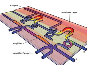
An artist’s conception illustrates a 3-D hybrid structure with
nonlinear and passive optical elements, enabling all-optical signal processing.
Courtesy of Barry Luther-Davies, Australian National University.
“We believe this will lead to a practical method by which
nanowires can be combined with more conventional circuitry without facing insurmountable
alignment challenges that accompany the more conventional approach to hybrid circuitry,”
Luther-Davies said.
A final example of nonlinear optical processing comes from the
University of Stuttgart in Germany, where researchers demonstrated an all-optical
control scheme of a hybrid plasmonic-photonics system, with their approach exploiting
a nonlinear third-harmonic-generation process.
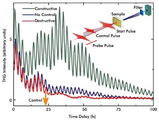
Using a control pulse injected after a start pulse, researchers demonstrated
all-optical control of a plasmonic mode, raising the possibility of creating a whole
new class of all-optical computers. Courtesy of Tobias Utikal, University of Stuttgart.
They did so by firing a sub-10-fs near-infrared laser pulse into
a metal structure sitting on top of a quartz substrate. The metal was fabricated
in 100-nm-wide ridges spaced 530 nm center to center.
The first pulse excited a polariton polarization in the nanostructure.
The investigators then fired a second pulse into the device a few tens of femtoseconds
later. This one either turned off the polarization or enhanced it, depending upon
the length of the delay. To probe what was going on, they used a third pulse.
Tobias Utikal, a graduate student, was lead author of a March
2010 Physics Review Letters paper that described this approach. He noted that plasmonic
structures could form the basis for all-optical nano-devices upon which an entirely
new class of computers could be built.
This is a possibility because plasmonic structures combine optical
responses in the femtosecond time range with nanoscale-size electric fields. Right
now, however, such computers are a long way off, partly because there currently
is no way to predict the nonlinear behavior of plasmonic devices.
Thus, one of the goals is to develop the knowledge needed so that
devices can be designed for the lowest power and highest speed switching. When and
if that happens, the results obtained by the Stuttgart researchers in their three-pulse
setup could provide a scheme for building these devices.
As Utikal said, “The results show that the plasmon can indeed
be switched off or reamplified at any time after its excitation. This method might
be utilized in the future in active plasmonic devices for ultrafast optical switching.”