The race is on to develop the next
technology that will enable manufacturers to continue scaling down their chip sizes.
Will optics provide the answer everyone is looking for?
The brisk march of optical lithography has set the pace for the
shrinking size of semiconductor devices and integrated circuits (ICs) that we see
today. Optical lithography – the technology of patterning – enables
intricate circuits to be created in wafers at dimensions smaller than the light
wavelength used in the process.
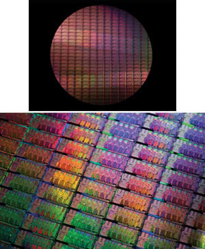
Optical lithography enables Intel to build state-of-the art chips
with feature sizes as small as 32 nm and below. As lithography systems progress,
integrated circuits can be made with more performance and more features, better
power efficiency and lower cost per transistor. Images courtesy of Intel Corp.
As ever shorter wavelength sources are developed, the resolution
of patterning continues to improve, and circuit features can shrink. But some believe
this progress is starting to slow, threatening the perpetuation of Moore’s
Law.
Moore’s Law was formulated by the co-founder of Intel, Gordon
Moore, in 1965, when he predicted that the number of transistors that can be placed
on an IC would double every year. He later revised this to approximately every two
years.
Keeping up with Moore’s Law over the past four decades has
seen lithography wavelengths drop from the 436 and 365 nm produced by mercury arc
lamps to 248 nm by the krypton fluoride excimer laser. In 1998, a group at MIT’s
Lincoln Laboratory developed a 193-nm source with the argon fluoride laser, which
is used to produce today’s 45- and 32-nm IC technologies.
Despite the trend in reducing exposure wavelengths, today’s
aggressive feature sizes are still falling farther and farther below the available
exposure sources, complicating the imaging challenges.
But the biggest question in the field today is this: What imaging
method will be used to pattern features that are 22 nm and below? Will shorter wavelengths
such as the long-awaited extreme-ultra-violet (EUV) be the answer, or can Moore’s
Law be extended by other means?
Optical lithography equipment
It is time to consider some of the other optical elements in a
lithographic system. In the quest to create smaller chips, manufacturers have developed
phase shift masks, improved the chemistry of photo-resists and fabricated lenses
with very high numerical apertures (NAs) and near-diffraction-limited performance.
The technique employed by most modern optical lithography equipment
is known as projection printing. In the setup, laser light shines through a mask,
which contains the pattern to be imaged onto the wafer. But the large gap between
the mask and the wafer results in diffraction, effectively spreading out the laser
light.
A well-designed objective lens is used to gather the diffracted
light from the mask before it is projected onto the wafer, whereby the ability of
the lens to collect diffracted light is measured by its NA.
Although using a lens with a higher NA results in better resolution
of the image, there is a price: As the NA increases, the depth of focus decreases.
Poor depth of focus could cause some points of the wafer to be out of focus; increased
NA also requires the wafer to be positioned extremely precisely.
“Optical lithography is the art of printing as close to
the Rayleigh limit as possible while maintaining a high level of uniformity and
stability for high-volume manufacturing. Maintaining fidelity of the pattern to
be printed is also extremely difficult, and it deteriorates the closer one prints
to the Rayleigh limit,” said Sam Sivakumar, Intel fellow and director of the
lithography technology and manufacturing group there.
One of the ways Intel tackled the dilemma involved the introduction
of phase shift masks, which began with its 45-nm node to increase the effective
contrast. Intel pioneered the use of alternating phase shift masks (starting at
90 nm) and attenuating phase shift masks (starting at 130 nm). The company also
introduced extensive optical tailoring of substrate materials to deliver specific
optical performance in aid of the patterning needed.
“Today’s lithography process is a highly optimized
and fine-tuned mixture of techniques to enable Moore’s Law scaling,”
Sivakumar said. “Phase shift masks have become ubiquitous. Source optimization
has become highly sophisticated with the advent of diffractive optical element sources.
Finally, photoresist chemistry has become increasingly sophisticated, enabling much
higher resolution and fidelity.”
Another trick of the trade makes use of the refraction caused
by water. The process, known as immersion lithography, is used by the industry today
for state-of-the-art processes. It effectively reduces the wavelength by about 30
percent. Intel started using this technique at 32 nm, and others followed at 45
nm.
Progression, but not at any price
But Moore’s Law isn’t just about getting more transistors
on each chip; it’s also about bringing down the cost of transistors. Optical
lithography equipment has so far met industry demands, but to preserve the law,
a new advance is needed soon.
EUV lithography has been the much anticipated solution; however,
its development has proved to be far from smooth, causing some in the industry to
lose faith. Developing a source in this regime that is powerful, robust and stable
enough for a modern semiconductor fab is a huge challenge, and there has been disappointment
over its progress.
According to Dr. Michael Fritze, director of Disruptive Electronics
at the University of Southern California Information Sciences Institute in Marina
del Rey, a process known as double patterning is now being considered as a candidate
for feature sizes below 32 nm. The technique is a complicated and expensive method
of doubling up the layers of printing, but Fritze believes that this will be the
most likely solution until EUV is finally ready.
The problem with both EUV and double patterning lithography solutions
is the cost, and the semiconductor industry has not been keen to implement the techniques.
For most fabrication facilities, it takes billions of dollars to create the fab
and then substantial amounts of money to maintain the capability.
This is where DARPA believes it can fit in with its three-year
GRATE (Gratings of Regular Arrays and Trim Exposures) program, which kicked off
at the end of 2010. The goal of GRATE is to develop methodologies enabling simplified
circuit designs using high-resolution grating patterns that can be fabricated using
either mask-based or maskless interference lithography.
Previously headed up by Fritze while he was program manager at
DARPA, the program is now led by Dr. Carl McCants, who explained that the vision
is to make low-volume fabrication at advanced nodes affordable for the US Department
of Defense (DoD).
“If it becomes cost-ineffective to implement in a given
technology, people will stop,” McCants said. “Large companies can absorb
the cost of development, but the DoD is looking for advanced technology access for
low-volume manufacturing.”
While this program is set to benefit low-volume fabrication, specifically
of custom silicon-based application-specific integrated circuits, high-volume manufacturers
must look elsewhere.
Despite its problems, EUV lithography is still being pursued and
heavily invested in by many R&D departments, including Globalfoundries of Milpitas,
Calif., which was the first company to produce working memory cells using EUV lithography.
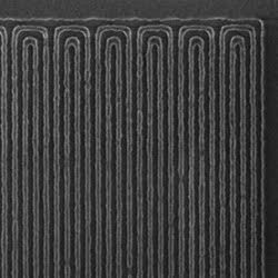
A scanning electron micrograph image of a
56-nm pitch pattern in resist, exposed on an EUV Alpha Demo Tool using a Globalfoundries
mask. Credit: Harry Levinson, Globalfoundries.
“We were leaders in the initial development phases of EUV,
and we plan to extend this leadership position as the technology approaches maturity,
including being one of the first customers for a production-level EUV tool,”
said Harry Levinson, senior fellow and manager of strategic lithography technology
there.
Lithography systems maker ASML of Veldhoven, the Netherlands,
continues to ship its preproduction EUV machine, NXE:3100, with the aim of refining
the technology in time for high-volume chip production starting in 2013.
Meanwhile, Intel is hedging its bets, working on a variety of
techniques to extend 193-nm lithography and to develop EUV lithography.