Dr. Colin Coates, Andor Technology PLC
Since the launch in late 2010 of imaging
cameras based on a new 5.5-megapixel scientific CMOS (sCMOS) sensor, there has been
much speculation about whether sCMOS will become a technology replacement for interline
CCD and electron-multiplying CCD (EMCCD) cameras, in many ways considered the current
gold standard for low-light fluorescence microscopy and other bioimaging techniques.
Coming from the unique market position of manufacturing all of the aforementioned
camera types, we provide here a comparison of these sensitive imaging technologies.
Technology overview
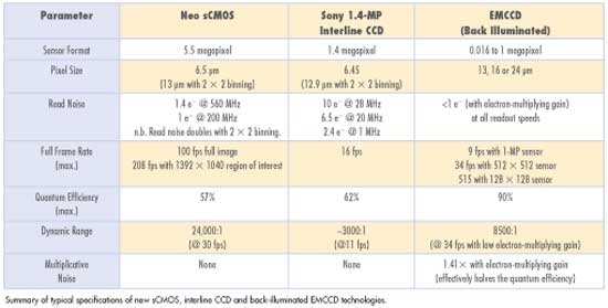
The small-pixel interline CCD has dominated bioimaging for more
than a decade. For cell microscopy, the leading sensor type has been a 1.4-megapixel
format from Sony, offering 5 to 6 e− read noise at approximately 11 fps (down
to 2.4 e− at 1 fps). The 6.45-μm pixel size represents a distinct “sweet
spot” – an ideal balance between the photon collection area per pixel
and the ability to oversample the diffraction limit for better resolution of fine
intracellular detail.
The EMCCD camera was introduced to the scientific market by Andor
in 2000 and represents a significant leap forward in combining ultrasensitivity
with speed.1 EMCCD cameras employ an on-chip amplification mechanism called “impact
ionization” that multiplies even single-photon events well above the read
noise floor. Importantly, this renders the EMCCD capable of single-photon sensitivity
at fast frame rates. This attribute has rapidly gained recognition for EMCCD technology
in demanding ultralow-light measurements, such as single-molecule detection and
photon counting experiments.
Although a well-optimized EMCCD is close to a “zero noise
floor” detector, the downside is that the signal amplification mechanism carries
an additional noise source called multiplicative noise, which effectively increases
the shot noise, or Poisson noise, of the signal by a factor of 1.41. This is manifested
as an increase in the pixel-to-pixel and frame-to-frame variability of signals.
Furthermore, the popular back-illuminated EMCCD sensors are limited to a smallest
pixel size of 13 μm. Although this size offers a good photon-collection area,
it tends to limit the ability to resolve intracellular detail.
As for sCMOS technology, it is based on a new generation of CMOS
design and process technology. This device type carries an advanced set of performance
features that renders it entirely suited to high-fidelity, quantitative scientific
measurement. sCMOS can be considered unique in its ability to simultaneously deliver
on many key performance parameters while also overcoming the performance drawbacks
typically associated with conventional CMOS imagers.
The 5.5-megapixel sensor offers a large field of view and high
resolution without compromising read noise or frame rate, and a 6.5-μm-pixel
size is again ideally suited to cell microscopy. The read noise is exceptionally
low, even when compared with the highest-performance slow CCDs, but not as low
as the effective read noise of EMCCDs. The sCMOS device can achieve down to 1 e−
rms read noise without amplification while reading out 5.5 megapixels at 30 fps.
Furthermore, the sensor can achieve 100 full fps with a read noise of 1.4 e−
rms.
Significantly, under extremely low light conditions, an sCMOS
camera can be readily operated with pixel binning, creating larger “superpixels”
for improved photon collection when required. It is worth noting that, unlike with
interline CCDs, under this 2 x 2 binning condition, the read noise of sCMOS will
double; that is, 1 e− rms becomes 2 e− rms. This noise increase is appropriately
factored into comparative signal-to-noise ratio (SNR) plots shown in this article.
By way of a unique dual-amplifier sensor architecture, the sCMOS
camera offers much higher dynamic range than would be expected from a CCD with a
similarly small pixel size. This design circumvents the need to choose between high
or low gain amplifiers, in that signal can be sampled simultaneously by both high
and low gain amplifiers. As such, the lowest noise of the sensor can be harnessed
alongside the maximum well depth, affording the widest possible dynamic range.
The sCMOS can read out in both “rolling” and “global”
(snapshot) shutter modes.2 Dark signal generated in each mode is similar, but the
absolute fastest frame rates and lowest read noise can be achieved in rolling shutter
mode, which will suit the vast majority of biological imaging applications, because
objects will typically move subpixel distances during the time taken for rolling
readout to traverse them.
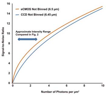
Figure 1. Plots comparing SNR of sCMOS versus interline CCD cameras
(neither with pixel binning) as a function of incident photons per square micron
on the sensor. sCMOS provides higher SNR throughout the intensity range because
of a significantly lower read noise floor. The specifications for sCMOS are based
on the Andor Neo camera, operated in rolling shutter mode with 560-MHz readout speed
and fan-cooled to –30 °C. The CCD interline performance is based on the specifications
of the Andor Clara camera at 20-MHz readout speed and fan-cooled to –55 °C.
Exposures of 1 s are assumed, such that the dark signal contribution from each cooled
camera is relatively small. Images courtesy of Andor Technology plc.
Sensitivity comparisons
Figure 1 shows a plot of SNR against number of photons per μm2
for sCMOS vs. interline CCD camera technologies. The X-axis is a representation
of photon flux incident on the detector surface; a value of 1 equates to approximately
42 photons incident within a 6.5-μm pixel. Between the two technology types,
the read noise difference is reflected in the notable separation between the respective
SNR curves across the intensity range shown. Figure 2 demonstrates clear distinction
in low-light-signal contrast, arising from read noise differences between sCMOS
and interline CCD cameras. The comparative images were recorded on a spinning disk
confocal fluorescence microscopy setup (an inherently low light modality), the signal
intensity ranging between 0.5 and 2.7 photons incident per μm2 of the sensor.

Figure 2. Comparative low-light images taken with Andor Neo sCMOS
(1.2 e− read noise at 400 MHz) versus Andor Clara interline CCD (5.5 e−
read noise at 20 MHz) of a fluorescently labeled fixed cell using a CSU-X spinning
disk confocal microscope (60x oil objective), each 100-ms exposure, same laser power
per channel, displayed with same relative intensity scaling. Note that the field
of view is limited by the aperture size of the CSU-X spinning disk unit, which is
matched to the 1.4-megapixel interline sensor.
Figure 3a shows a further plot of SNR against number of photons
per square micron, this time for sCMOS (nonbinned and 2 x 2 binned) versus a 13-μm
back-illuminated EMCCD camera, for which the zero to 10 photons per μm2 range
shown represents a relatively bright signal regime. Consideration of the curve for
2 x 2 binned sCMOS provides a keen perspective on just how effective the pixel size
becomes on the overall sensitivity performance. Across the range shown, the 2 x
2 binned sCMOS appears to exhibit a better SNR than a back-illuminated EMCCD camera
with equivalent pixel size (nonbinned). It is reasonable to ask why a “zero
read noise” back-illuminated EMCCD camera would exhibit lower SNR than a >2
e− noise (when binned) front-illuminated sCMOS device. The answer lies in
the additional multiplication noise imposed by the EMCCD signal amplification mechanism.
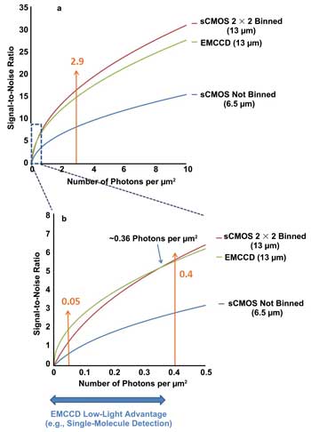
Figure 3. Plots comparing SNR of sCMOS (nonbinned and 2 x 2 binned) and larger-pixel EMCCD (nonbinned) as a function of incident photons per μm2 on the sensor. Two ranges
are given; the expanded low-light range (b) is where the “zero read noise”
operation of EMCCDs offers a distinct sensitivity advantage.
However, the light range shown does not emphasize the truly low
light signal intensities and associated applications whereby EMCCD technology will
provide an SNR advantage. Figure 3b shows the same data, but expanded on the low-light-
intensity range between zero and 0.5 photons per μm2 (i.e., up to ~85 photons
per 13-μm pixel). At signal intensities below 0.36 photons per μm2, the
back-illuminated EMCCD will offer an improved SNR compared with the 2 x 2 binned
sCMOS. This in effect is the region in which the “zero read noise” properties
of an EMCCD outweigh the negative effect of multiplication noise.
By way of demonstration, Figure 4 shows comparative images recorded
of an LED-illuminated resolution chart in a lighttight imaging chamber at a series
of light intensities, marked in the Figure 3 graphs. The images taken in the very
low light regime – below the “crossover” point – clearly
demonstrate the sensitivity advantage of the “zero read noise” EMCCD
in this range.

Figure 4. Comparative low-light images taken with Andor Neo sCMOS
(1.4 e− read noise at 560 MHz) versus Andor iXon3 888 back-illuminated EMCCD
(<1 e− read noise), under a range of photon intensity conditions, indicated
on the Figure 3 plots. sCMOS was 2 x 2 binned so as to have the same effective pixel
pitch (and light-collection area per pixel) as the 13-μm pixel of the EMCCD
sensor. The superior sensitivity of back-illuminated EMCCD under extremely low light
conditions is readily apparent.
Application decisions
Such raw sensitivity performance at extremely low light signal
intensities means that EMCCD technology will still be the detector of choice for
a number of demanding applications. For example, the principal microscopy usage
of EMCCDs to date has been in single-molecule biophysics, and this is unlikely to
change significantly. An exception may become apparent in the area of superresolution
microscopy by single-molecule localization techniques (e.g., PALM, STORM). Because
this approach is required to reach a threshold SNR to yield sufficient localization
accuracy, the corresponding number of photons per exposure required may occur at
or beyond the crossover region between the two technology curves.
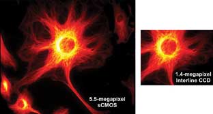
Figure 5. Field-of-view comparison of two technologies at 60x magnification.
1.25-NA, 5.5-megapixel sCMOS versus 1.4-megapixel interline CCD (each has ~6.5-μm
pixel pitch). sCMOS can offer this larger field of view at 100 fps with 1.4 e−
read noise.
Although the majority of live-cell microscopy experiments may
eventually opt to use sCMOS technology – particularly to benefit from the
6.5-μm pixel size combined with the larger field of view of the 5.5-megapixel
sensor – there will be some exceptionally low light instances in which a back-illuminated
EMCCD will remain indispensable, for example, when measuring calcium flux from smooth
muscle cells using the Nipkow spinning disk confocal modality. Furthermore, because
sCMOSs are not single-photon-sensitive, EMCCD technology is still required for single-photon-counting experiments.
Considering the sCMOS vs. interline evidence, it seems more likely
that interline CCD technology eventually will be displaced by sCMOS technology,
especially in the field of cell microscopy, but also in other applications, such
as high-throughput genome sequencing, high-content screening and ophthalmology.
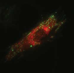
Figure 6. Mouse embryonic fibroblast cells transfected with DNA plasmids,
encoding for two fluorescent proteins: clathrin, fused to green fluorescent protein
(GFP-clathrin), and Rab5, fused to the monomeric red fluorescent protein (mRFP-Rab5),
imaged by total internal reflection fluorescence microscopy. GFP-clathrin localizes
to vesicles that form on the plasma membrane of cells (visible as green spots).
mRFP-Rab5 is found on vesicles located more internally but still within the evanescent
field generated by total internal reflection fluorescence (red spots). Images courtesy
of Dr. Roberto Zoncu, Whitehead Institute for Biomedical Research, MIT.
One exception remains, whereby a cooled interline CCD maintains
an application advantage over a cooled sCMOS camera. This relates to long-exposure
luminescence detection; e.g., bioluminescence microscopy, chemiluminescence gel
documentation or in vivo bioluminescence imaging. In those applications, exposures
greater than 60 s will yield a lower overall noise floor (read noise and dark noise
combined) for the Sony interline CCD. There are two reasons for this: (a) at rates
slower than 1 fps, the Andor Clara interline readout can be reduced to 1 MHz, which
reduces the read noise to ~2.4 e−; (b) a cooled Sony interline sensor maintains
an extremely low dark current performance relative to cooled sCMOS. Performance
comparisons aside, the more general reality is that interline CCDs will most likely
continue in the market for some time because of cost advantage.
Ultimately, however, we are witnessing the early stages of product
entry, and the ink is still wet regarding which applications will truly benefit
from switching to sCMOS technology. However, the material presented here should
prove beneficial, at least in making an informed decision about whether to evaluate
any of the detection solutions covered.
Meet the author
Dr. Colin Coates is product manager at Andor Technology plc in
Belfast, UK; e-mail: [email protected].
References
1. M. Hollywood et al (Nov/Dec 2004). Optimizing low-light microscopy
with back-illuminated electron multiplying charge-coupled device: Enhanced sensitivity,
speed, and resolution. Journal of Biomedical Optics, pp. 1244-1252.
2. B. Fowler et al (January 2010). A 5.5Mpixel 100 frames/sec
wide dynamic range low noise CMOS image sensor for scientific applications. Proc.
SPIE, 7536, 753607.