by Caren B. Les, Staff Editor
A rapidly growing branch of physics promises all-optical computer chips and ultrafast computing speeds.
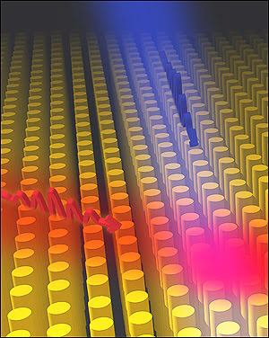
An artistic impression of light interaction in plasmonic nanorod metamaterial. Researchers are working to use plasmonic metamaterials to guide light in applications such as superhigh-speed computing. The science of plasmonics involves the interaction of light and metal at the nanoscale. (Photo courtesy of Ryan McCarron, www.activeplasmonics.org)
Plasmonics, also called “light on a wire,” exploits the nanoscale interaction of light and metal and is a focus of research in the optical sciences, photonics, thin films and nanotechnology. The science has many possible applications, including in biosensors for healthcare, in light concentration for solar energy, and in optical instrumentation for performing research. Scientists say that plasmonic technology could enable the creation of a microscope lens that can resolve nanoscale objects with visible light.; it also could be used as an “invisibility cloak” to hide objects.
Researchers have constructed plasmonic devices — basically nanoscale metal structures — to guide and direct light. The technology combines the ultrahigh speed data transfer benefits of fiber optics, with the small size and other advantages of electronic components. Two teams recently published papers on technical advances in the field.
Anatoly Zayats, a professor at King’s College London, leads a team looking at optical components for superfast computing, and Xiang Zhang, a principal investigator at the US Department of Energy’s Lawrence Berkeley National Laboratory and the University of California, Berkeley, and his team work in the area of gradient index (GRIN) lenses.
Metamaterials: Guiding the light
Zayats and his team reported an advance toward developing optical components for superfast computers and high-speed Internet services, which they say could revolutionize data processing speeds by transmitting information via light rather than through electric currents.
The scientists have designed an artificial material similar to a stack of nanoscale rods that allows light beams to interact efficiently and change intensity — allowing information to be sorted by beams of light and very high speeds, solving the difficulty of light beams interacting with one other while they travel through a material.
This metamaterial reportedly could be incorporated into existing electron chips or it could be used to build completely new all-optical chips that could revolutionize data processing speeds. The scientists showed that closely spaced plasmonic gold nanorods produced an ultrafast transmission change when they were illuminated with a low-energy optical pulse, according to a press release from the Argonne National Laboratory in Illinois, which also participated in the research.
The main discovery is that nanorod material exhibits nonlocality of the optical response, which has an unusually strong linear dependence on incident light intensity.
Zayats recently expanded upon key elements of the research and what lies beyond.
Q: How would you describe your recent advance in metamaterials and how it relates to high speed computing and enhanced Internet services?
Zayats: Currently the information in computers is processed in the form of electric signals. The speed [at] which you can send signals along tiny electric interconnects within a chip or between chips is limited due to [the] small size of the electric interconnect. If optical signals can be used, the speed can be increased. But then optical signals need to be sent along tiny waveguides.
Broadband Internet already uses light to transmit the information along optical fibers but when it comes to active manipulation of the information (to send the signal along one fiber or another), these optical signals first converted to electric signals, routed in one or another channel and optical signals are generated again. This naturally introduces delays and additional power consumption.
If one can manipulate optical signals without converting them into electric and back this would provide significant improvement in the speed of information processing. In order to achieve this, one needs the so-called nonlinear optical materials which enable interaction between the light wave carrying signal and the control light. The efficiency of the interaction is very small and in order to control light with light one needs devices of large size and/or very high light intensity.
Using the metamaterial approach we have engineered nonlinear material that has a very strong effective nonlinearity and can enable control of light by light at very low intensities.
Q: How do you expect the advance will contribute to improved computing and high speed Internet?
Zayats: The developed metamaterial needs to be integrated with photonic waveguides and then the resulting devices will be able to perform all optical modulation and switching of photonic signals without the need to convert the signal from optical to electric and back.
Q: What would you say is currently happening in the area of plasmonics and plasmonic devices for computers and Internet technology? Would you describe some specific plasmonic devices you are working on for these applications?
Zayats: After several very fruitful years for plasmonics in terms of basic research, now it comes to hard engineering work to develop really integrated components that can be used for building advanced photonic circuits. Many groups are working on various implementations starting from simpler designs using thermo-optical effects, going to electro-optical control and all-optical photonic circuitry.
Integration of plasmonic components within standard photonic circuitry and indeed with silicon photonics is on the agenda and will boost practical introduction of plasmonics in real life devices.
Advances in hybrid plasmonic devices resulted in significant progress in overcoming the propagation losses of plasmonic circuitry and indeed achieving plasmonic-based nanolasers (the so-called spasers) that can be used as nanoscale light sources that can be directly integrated on electronic chips.
Q: In your opinion, what further work needs to be done in the area of plasmonics and computing?
Zayats: Specifically for optical information processing, the main point of concern is energy requirements — one needs as small [an amount of] energy per bit as possible. With the metamaterial that we have developed the switching can be achieved with few tens of femtojoules in about 100-nanometers-size components. Additional improvement by 10 times in both size and energy is very much desirable for practical use.
“The first commercial products were available back in 2002 but it came very unfortunately just before the telecom crash and this obviously slowed things down, Zayats further noted. “Now 10 years later, people are more cautious trying an approach marked with more integrated solutions rather than individual components.” The next significant commercial success for plasmonics will probably be in data storage, rather than in computing itself, he said.
The work of Zayats and his group was published online in the journal Nature Nanotechnology on January 23, 2011. The paper is titled “Designed Ultrafast Optical Nonlinearity in a Plasmonic Nanorod Metamaterial Enhanced by Nonlocality.”
Other members of Zayat’s team involved in this research were from the University of South Florida, in Jacksonville, the University of Massachusetts at Lowell, and Queen’s University of Belfast,Northern Ireland.
GRIN lenses: Routing the nanoscale light
“Our GRIN plasmonics technique provides a practical way for routing light at very small scales and producing functional plasmonic devices,” said Xiang Zhang. GRIN plasmonics combines methodologies from transformation optics and plasmonics. In transformation optics, the physical space through which light travels is warped to control the light’s path. In plasmonics, light is confined in dimensions smaller than the wavelength of photons in free space, making it possible to match the different length-scales associated with photonics and electronics in a single nanoscale device, according to the press release.
Zhang and his team at the Berkeley Lab and the University of California, Berkeley, have carried out an experimental demonstration of the hybrid technology that the researchers say could open doors to innovative optics, including superfast computers based on light, optical microscopes able to resolve DNA molecules with visible light, and “invisibility cloak” devices.
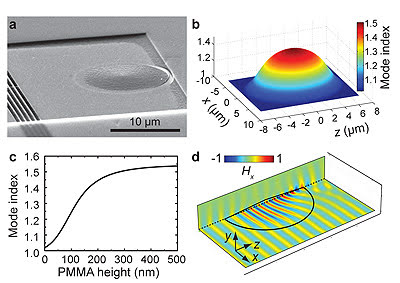
Scanning electron microscope image of a plasmonic Luneburg lens, which could have applications in high-speed computing. Developed by researcher Xiang Zhang and his group in Berkeley, Calif., the lens is made of poly (methyl methacrylate) (PMMA) on top of a gold film (lens diameter, 13 mm). Zhang said that he and his group demonstrated that the Luneburg lens can focus surface plasmon polaritons (SPPs). b, Mode index (vertical axis) for the Luneburg lens at a wavelength of 810 nm. c, Relation between PMMA height and mode index for SPPs on a gold surface at a wavelength of 810 nm. d, Cross-sections of the normalized magnetic field Hx (at the metal–dielectric interface in the x–z plane and for x¼0 in the y–z plane) for SPPs propagating through the Luneburg lens in the positive z-direction. (Photo courtesy of Nature Publishing Group)
The researchers fabricated highly efficient plasmonic versions of Luneburg and Eaton lenses, according to a press release from the Berkeley Lab. A Luneberg lens focuses on light from all directions equally well, while an Eaton lens bends light 90° for all incoming directions. They worked with composites featuring a dielectric (nonconducting) material on a metal substrate, and “grey scale” electron beam lithography, a method used for patterning 3-D surface topographies in the computer chip industry.
“Applying transformation optics to plasmonics allows for precise control of strongly confined light waves in the context of two-dimensional optics,” said Zhang.
“Plasmonics takes advantage of the properties of surface plasmon polaritons (SPPs), which are localized or propagating quasi-particles in which photons are coupled to the quasi-free electrons in metals,” according the group’s paper titled “Plasmonic Luneberg and Eaton Lenses,” published online in Nature Nanotechnology on Jan. 23, 2011.
Zhang recently shared his thoughts on the group’s findings, and on the outlook for the field.
Q: How will your team’s advance contribute to enhanced computing and information technology, (and other major application areas)?
Zhang: Our approach is useful for downscaling optical computing devices. As we know, optical computing promises high speed and low power consumption compared with semiconductor-based electronic computers. However, conventional optics suffers from the fundamental diffraction limit, meaning we cannot confine light to dimensions smaller than half wavelength. Plasmonics can overcome such a limit, and enable [us] to confine, guide and manipulate light at the deep subwavelength scale. Therefore, it is possible that we can build ultrasmall and ultrafast computers based on the new hybrid GRIN plasmonics techniques. Meanwhile, plasmonic waves can carry both electronic and optical signals. We may find a hybrid version of the computing devices combining the strength of both the nanoelectronic and photonic technologies. Other applications may include efficient photovoltaics, ultrasensitive biomedical detection, high-resolution microscopy/lithography, and so on.
Q: How would you describe your new hybrid GRIN plasmonics techniques, which combine methodologies from plasmonics and transformational optics? What specifically makes this technology cutting edge? What do you consider the most important aspects of your research findings?
Zhang: There are several unique properties and advantages of our technique. First, our approach nicely bridges plasmonics and transformation optics, two very active research areas. Using this very general method, we can realize more advanced, complex plasmonic elements with superior performance.
Second, our method provides a practical means to efficiently manipulate SPPs with low scattering losses. Our work demonstrates that we can manipulate SPP propagation by continuously tailoring the thickness of an isotropic dielectric cladding layer on top of a metal. It is in sharp contrast to previous plasmonic devices, which were realized by structuring the metal surface or adding discrete scattering structures on the metal. In this case, the scattering losses due to discontinues of geometries or materials are very large. In contrast, our approach leads the surface wave to pass through a “soft transition” into the element which strongly reduces reflection/scattering of the otherwise discrete interface.
This is similar to an antireflection coating used on goggles or glass surfaces.
Third, our method is fully compatible with active plasmonics. The loss could be reduced even further by incorporating various gain materials, such as quantum dots and fluorescence dye molecules into the dielectric cladding layer, further increasing propagation distance of SPPs required for plasmonic interconnects or even all-optical devices.

A demonstration of a plasmonic Eaton lens. Zhang and his group showed that this lens can function as a surface plasmon polariton (SPP) waveguide bend with low bending losses. a, A scanning electron microscope image of an array of Eaton lenses on top of a gold film. b, Height profile cross-section for the left side of the lens measured by atomic force microscopy (solid line) compared to the model (dashed line). c,d, Fluorescence microscopy image and corresponding simulation of the fluorescence intensity of the Eaton lens for SPPs propagating in the positive z-direction and bending to the right side when passing through the lens. Arrows indicate the launching position and direction of the SPPs. Solid lines mark the outer diameter of the lens and dashed lines the high index region, which was set to 1.54. In the color scale, black represents low intensities and yellow high intensities. (Photo courtesy of Nature Publishing Group)
Q: What generally will need to be done before the plasmonic versions of Luneberg and Eaton lens technology can be brought to market?
Zhang: We have demonstrated that the Luneburg lens can focus SPPs, and the Eaton lens functions as an SPP waveguide bend with low bending losses. Both of them are important nanoplasmonic elements. Although the design and fabrication methods are quite general and can be easily extended to mass production, we need to think more about where and how to use these plasmonic devices. One potential application may be plasmonic photovoltaics.
Q: What would you say are the main challenges to designing and fabricating plasmonic devices for superfast computing, data transmission and other areas of information technology?
Zhang: One major challenge is the loss problem inherent to all plasmonic devices. There are two sources of the loss. The first one is the intrinsic Ohm loss of metals, leading to energy dissipation into heat when plasmonic waves/signals transmit. The second one is scattering loss due to structure imperfection and/or topology discontinues, which gives rise to the re-radiation of plasmon waves into far-field propagating waves. Our GRIN plasmonic technique can help to suppress the scattering loss. For the Ohm loss, we need to seek better metals/alloys, or use gain materials to compensate the Ohm loss. This is a very challenging task, but we already saw some progress along this direction.
Q: What is the next step for you and your team in this area of research?
Zhang: We are working on more complex plasmonic devices in combination with transformation optics, such as plasmonic collimators, single plasmonic elements with multiple functions, and plasmonic lenses with enhanced performance.
Q: What would you say is currently happening in the area of plasmonics and plasmonic devices for computers and internet technology? What other developments might we see in this area of research in the next few years?
Zhang: Definitely it is an infant area. We haven’t seen many breakthroughs of plasmonics in the area of optical computing/information. But we think it is an extremely exciting and fascinating direction to pursue. With the advanced design, modeling and fabrication technique, it is very promising to achieve some significant developments in the next few years.
New Quasiparticles for Optical Computing
Zhang and researchers at the Berkeley Lab have also created a new quasiparticle called a “hybrid plasmon polariton,” which they say could open the doors for integrated photonics circuits and optical computing. They have demonstrated the first true nanoscale waveguides for next-generation on-chip optical computing systems, according to a May 2011 press release from the Berkeley Lab.
“The novel mode design of our nanoscale waveguide holds great potential for nanoscale photonic applications, such as intra-chip optical communications, signal modulation, nanoscale lasers and biomedical sensing.” said Zhang.
A paper published by Nature Communications on May 31, 2011, titled “Experimental Demonstration of Low-Loss Optical Waveguiding at Deep Subwavelength Scales” details this work.
Conference Keynotes
Keynote presenters Zhang and Zayats will discuss the latest progress in nanoplasmonics at a conference on the topic to be held within the NanoScience+Engineering segment of SPIE’s 2011 Optics+Photonics meeting in San Diego in August.
[email protected]