Martin Hünten, Daniel Hollstegge, Yang Wang, Reik Krappig, Olaf Dambon and Fritz Klocke, Fraunhofer Institute for Production Technology IPT
An EU-funded research project aims to level out a new path for the optics industry in producing glass micro-optics.
The growing demand for compact technical products and the miniaturization trend are two developments that are exerting a major influence on the production of micro-optical components. The consumer industry, telecommunications and laser technology all rely on complex optics for a variety of products. Several methods for manufacturing such micro-optics have established themselves on the market over the past years. To close the gaps between the production methods, a consortium of 10 partners from six European countries has formed a research project called WaferLevelOptics.
Glass optics traditionally are produced in a range of forms using a series of grinding and polishing methods.1 However, this approach is not suited to larger quantities because the costs incurred from longer processing times in the machine and from the number of handling stages are too high. Consumer buying decisions are based primarily on price.
To provide high-quality glass optics under these conditions, manufacturers have for several years now counted on replicative technologies.2,3 Precision optics – as used in cameras or medical equipment, for example – are produced using precision molding, an established manufacturing method.
Plastic optics can be produced inexpensively using various replication methods. Wafer-based manufacturing, in which hundreds of small plastic optics can be modeled on a large glass wafer that measures up to 300 mm, has prevailed in the past (Figure 1). Various wafers can be assembled into optical systems and mounted.4
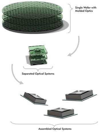
Figure 1. Principle of wafer-based optics manufacturing. Images courtesy of Fraunhofer Institute for Production Technology IPT.
However, for a growing number of applications, the properties of plastic optics are not sufficient, so precision optics must be made of glass. Small glass optics can be produced in the form of wafers but – so far – only if they are made of quartz glass. There are limitations to the dimensions of the individual lens, also; otherwise, the cost of etching cannot be justified.
This means that a gap exists from the point of view of production technology. Until now, it has not been possible to produce wafer-based micro-optics that were made of other types of optical glass, or with dimensions between 0.5 and 5 mm.
The WaferLevelOptics project, spearheaded by the Fraunhofer Institute for Production Technology IPT of Aachen, Germany, beginning in the fall of 2010, seeks to close this gap by developing the necessary technologies and methods. The project’s partners want to show that wafer-based production of a variety of glass optics is possible. A number of optics will be pressed onto a 100-mm glass wafer for demonstration and tested on the basis of practical examples.
As with other production technologies, precision molding is distinguished by a complex process chain. A sequence of many intricate steps, all occurring simultaneously, must be controlled to achieve success. For this reason, the focus of the WaferLevelOptics project is on developing the individual steps and amalgamating them into a complete process chain.
Optical design
The foundation for successful micro-optics components manufacturing is laid in the early phases, when the optics must be designed with replicative production in mind. Various manufacturers offer a wide range of optical glass, but not all of these are equally suited to precision molding. The Finnish research facility VTT (Technical Research Centre of Finland) is designing the optics for the project, giving careful consideration to the limitations of the molding process.
In turn, the optical designer thinks of new ideas, such as selecting spherical or aspherical components that can be implemented as both concave and convex. Distance elements between two individual optics can also be directly replicated during the molding process. The work required for alignment and handling is reduced in comparison to plastic optical systems, which must have their distance elements procured from elsewhere (Figure 2). The initial project results show that the distance elements within the molding process can be pressed onto the actual optics.
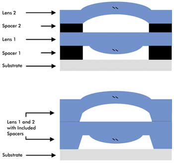
Figure 2. Multilens wafer-based systems with various approaches in relation to replicated lenses and wafers are shown. The optical system above has separate spacers, while the spacers are included in the optical system below.
Mold design, process simulation
Molding optical glass of any type requires temperatures of up to 800 °C. Therefore, the metals used in replicative manufacturing of plastic optics are not suitable as materials for molds. But ceramic materials and hard metals without binders can be used for precision molding. In the WaferLevelOptics project, these are developed and supplied by Ceratizit Luxembourg SARL. The process involved in using these materials does, nevertheless, present huge challenges. Metallic materials may be machined using milling and turning processes, but ceramic materials require time-consuming grinding methods.
The optical component design also must be scaled at the wafer level. Simply transferring and scaling the optical function surfaces will not lead to successful results. The reason is that, during the molding process’s cooling phase, the glass wafer experiences local and global shrinkage, which not only changes the position of the lens but also influences its local geometrics.
The effects of shrinking could be gauged and remedied, but the cost would be so high that, in the end, the finished optics would no longer be affordable. In the WaferLevelOptics project, the glass wafer replication is tested using finite element method simulations on the computer (Figure 3). In this way, both the distance between the single lens on the wafer and local shrinkage can be detected on the micrometer scale. The calculated values are applied directly to tool manufacturing, so no expensive practical trials are required. Aixtooling GmbH of Aachen and Fraunhofer IPT are designing the molding tools and executing the finite element method simulation.
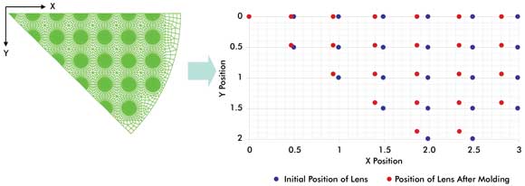
Figure 3. Simulation of global shrinkage in a 100-mm glass wafer. At left is the top view of a model of the finite element method; the graph on the right shows the lens position after the molding process.
Mold manufacturing
As with any replication process, the molding tool is the key to success. Because the contour and surface of the tool transfer precisely onto the glass, high surface quality and contour consistency are essential. The molding tool also adds the greatest cost.
Because producing ceramics for precision glass molding requires grinding, WaferLevelOptics must develop the processes and kinematics necessary to make these molds. Taking the machining process into account in detail and developing software solutions for programming the high-precision machines are essential factors. The aim is to set up a user-friendly software tool. This is where Aixtooling GmbH lends its expertise. Fraunhofer IPT is working on the mold manufacturing with System 3R International AB of Sweden.
Glass wafer replication
Precision-manufactured molds serve the purpose of pressing premanufactured and polished wafers made of various optical glasses in the subsequent replication process. It is important to inspect the molding process, to investigate how much force is required and to determine whether the two halves of the tool are aligned. Results so far show that only high-precision passive alignment and guide structures guarantee lateral overlapping of the tools in a single-digit micrometer range, along with minimal torsion.
The force with which very flat, large-surface wafers can be pressed is considerably greater than the force that must be applied for a single 1-mm-thick glass optical component with a 3-mm diameter. Replicating an individual component with the described dimensions requires a lower force by a factor of 1000 in comparison to a glass wafer with the same thickness but 100 mm in diameter. Standard glass molding machines can apply only limited force, so a compromise must be found. The force can be reduced when, for example, the glass is remolded at higher temperatures.
However, there are restrictions regarding this technique as well, because glass can be molded only within a limited temperature range. One partial aim of the WaferLevelOptics project is to find a suitable process layout for replicating 100-mm glass wafers with more than 100 individual micro-optics. Fraunhofer IPT is developing the molding process; Fisba Optik AG of Switzerland and Danish optics provider Kaleido Technology ApS will follow up with testing series production.
Alignment, connection, assembly
After replication, optical systems that contain more than one lens still must be mounted at wafer level. The individual wafers initially are stacked on top of each other and aligned with each other. To avoid having to manually align the optical components, as is still required in many cases, the project uses an automatic workstation that operates according to the principle of wavefront measurement. The wavefront of the individual optical system is measured and analyzed in transmission. On the basis of wavefront aberration, the rotatory and translational movements of the wafers relative to each other can be calculated and corrected. Trioptics GmbH is performing the necessary development work with support from Fraunhofer IPT.
Afterward, the aligned optical systems can be fixed and connected with the scheduled electronics at wafer level. Alternatively, the wafers can be cut into small, individual optics and systems and be added to other assemblies. Osram Opto Semiconductors GmbH and iC-Haus GmbH are integrating the optics in their model applications.
Outlook
The complete development work on wafer-based glass optics manufacturing and precision molding is being tested by the 10 members of the project consortium in specific, market-relevant applications. One of these consists of a collimation lens for LEDs; another approach targets a multilens system that can be used within a camera module. Both demand precise spherical and aspherical optical components made of glass that cannot yet be produced with the efficiency that the current status of technology requires.
Another intermediate aim on the path to a replicated 100-mm glass wafer is to mold optics initially into 50-mm glass substrates. The knowledge that has been gained and the developments that have been implemented can be used in the future as a basis for deploying 100-mm glass wafers bearing an even larger number of optical components.
Meet the authors
Martin Hünten, Daniel Hollstegge, Yang Wang and Reik Krappig are research assistants, Olaf Dambon is chief engineer, and Fritz Klocke is the director of Fraunhofer Institute for Production Technology IPT in Aachen, Germany; e-mail: martin.huenten@ ipt.fraunhofer.de.
References
1. V. Sinhoff (2009). Feinbearbeitung optischer gläser in der kleinserie. Dissertation. Aachen, Shaker, 1997.
2. A. Kunz (December 2009). “Aspheric freedoms” of glass. Optik & Photonik, pp. 46-48.
3. S. Nollau et al (2010). Designempfehlung für das präzisionsblankpressen. Photonik, Vol. 42, pp. 28-30.
4. M. Kast (December 2010). High-Precision Wafer-Level Optics Fabrication and Integration. Photonics Spectra, pp. 34-36.
For more information on the WaferLevelOptics project, visit: www.waferleveloptics.org.