 - High Performance Laser Modules 9/24 LB")
Plasma’s potential for photolithography pursued
Work over the past decade to harness the energy-generating mechanism of the sun has yielded bright high-energy light needed to etch smaller microchips.
The microchip industry now uses 193-nm UV light, which cannot etch circuits any smaller than those currently being made. The future standard for making microchips, the industry has determined, is 13.5-nm light. Creating such extreme-UV light requires high-temperature, electrically charged gases called plasma, but scientists have struggled to generate enough power with existing extreme-UV light sources.
“Over the past decade, the primary issue with these extreme-UV light sources is they just can’t produce enough power,” said Uri Shumlak, a University of Washington (UW) professor of aeronautics and astronautics. “It’s a stumbling block for the whole semiconductor industry.”
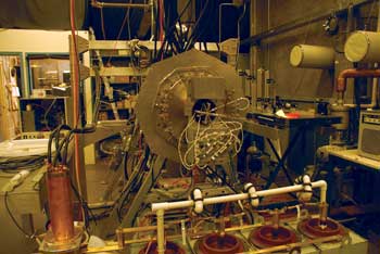
A new inexpensive fusion reactor model uses currents flowing through material, rather than giant magnets, to control the million-degree plasma that generates high-energy extreme-UV light for applications such as lithography. The lab experiment includes a small system that measures plasma for electronics applications, attached to a larger tank containing plasma for energy research.
The bright high-energy light developed by Shumlak and a UW colleague is a solution to this decade-long roadblock. The scientists developed an inexpensive fusion reactor model that uses currents flowing through the material, rather than giant magnets, to control the million-degree plasma that generates the high-energy light. The technique produces stable, long-lived plasma.
The researchers first conducted the experiment in 1999 and discovered a really bright light when they looked through the glass. They began to explore applications for this light and discovered a need in the microchip industry.
Existing technologies that are used to etch microchips produce sparks with a lifetime of 20 to 50 ns. The UW beam lasts 20 to 50 millionths of a second – about 1000 times longer. It also provides more control over the million-degree plasma that produces the light.
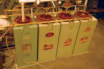
Four capacitors supply up to 10,000 V of energy to separate the xenon electrons from their nuclei, creating an electrically charged plasma that generates the high-energy light; the plasma created is stable and long-lived.
“That translates directly into more light output, more power depositing on the wafer, such that you can move it through in some reasonable amount of time,” Shumlak said.
The researchers demonstrated the method’s ability to generate 13.5-nm light with an initial grant from the university’s Center for Commercialization. They reduced the equipment from the size of a broomstick to the size of a pin that can generate a sharp beam, thanks in part to a Washington Research Foundation grant.
They have established a startup, Zplasma, to commercialize the technology for the next generation of microchip production.
Published: September 2012