Oliver Haupt, Dirk Müller and Frank Gäbler, Coherent Inc.
Many cutting-edge applications are critically enabled by ultrafast lasers, but other demanding applications can now switch to a new type of subnanosecond solid-state laser.
In recent years, Q-switched diode-pumped solid-state (DPSS) lasers and fiber lasers with pulse widths of a few tens of nanoseconds have become the workhorses for many micromachining applications. But some drilling, cutting and surface patterning applications demand even better results than nanosecond laser pulse widths can achieve. As a result, they have moved to lasers with picosecond pulse widths.
Ultrafast lasers can enable glass cutting for next-generation smartphone touch screens, and a new type of subnanosecond laser brings both performance and economy to some applications.
Why shorter pulse widths?
Pulse width is a critical parameter in micromachining applications – shorter pulse widths generally produce better results in terms of spatial resolution, depth control, edge quality and minimized peripheral thermal damage. One reason for this is that every material has an ablation threshold (the minimum peak intensity required to remove material).
For a given pulse energy, a shorter pulse is desirable because it is more efficient at material removal. Specifically, a shorter pulse delivers more of its total energy above this threshold power, where the absorption becomes increasingly nonlinear because of the higher electric field resulting from the higher peak power. In contrast, much of the energy of a longer pulse simply goes into heating the material.
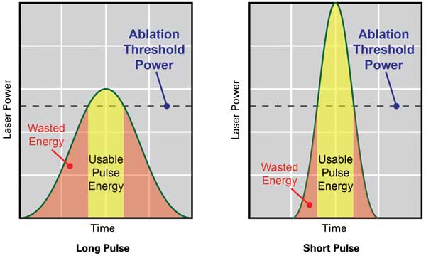
Figure 1. The effect of pulse width on machining with nanosecond lasers. With longer pulses, much of the pulse energy contributes only to heating – heat that can spread into surrounding material and cause damage known as the heat-affected zone (HAZ). With shorter pulses, a higher proportion of the pulse energy is delivered above the threshold power level, maximizing processing while minimizing the HAZ. Courtesy of Coherent.
Shorter pulse widths also mean that more of the deposited energy is carried away within the ejected material before thermal energy can flow into the surrounding material. This effect is most pronounced in thermal conductors such as metals, and slowest in thermal insulators such as plastics. As a reference point, in an intermediate material such as silicon dioxide, it can spread more than 1 µm in less than 10 ns. Achieving a submicron HAZ (heat-affected zone) therefore requires pulses shorter than 10 ns in this material.
When pulse widths get into the picosecond rather than nanosecond regime, peak powers become high enough to drive multiphoton absorption. This is a highly nonlinear effect in which interatomic bonds are directly broken through photoablation. So picosecond pulses remove material by a combination of this process and thermal ablation, rather than just relying on thermal ablation alone, as with nanosecond pulses. (Photoablation is possible with nanosecond lasers, but only by using higher-cost deep-UV photons – e.g., 193 nm.)
Photoablation is a relatively cold process with dramatically reduced peripheral thermal damage (Figure 2). And, because it is nonlinear, even visible and near-IR lasers can be used to process materials that are nominally transparent at these wavelengths.
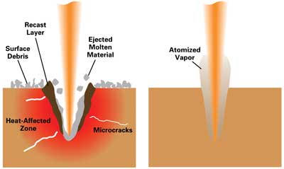
Figure 2. Nanosecond lasers drill or cut by heating and boiling off material. But ultrafast lasers remove material partly by a cold process called multiphoton absorption, which directly breaks the interatomic bonds. Their ultrashort pulse duration also serves to minimize any peripheral heating effects. Courtesy of Coherent.
However, although these ultrafast lasers can deliver significantly higher process quality, they machine at slower speeds than nanosecond lasers of the same average power rating. A key reason is that the cold ablation process involves breaking myriad individual bonds and breaking the material into constituent atoms via Coulomb repulsion. But with a thermal process, much of the material is ejected as small fragments or droplets; this requires less laser energy for the same amount of total material removal.
Cutting sapphire, glass for smartphones
Market demand for smartphones with increased functionality and ever-better displays has driven the need for laser micromachining, which enables numerous production processes, from stacked memory chips to display fabrication. For example, the ongoing push for thinner and lighter – yet also stronger – displays has created the need to cut very thin, strengthened glass using picosecond lasers.
A typical LCD touch screen contains four stacked layers of glass; the outer layer is currently a 700-µm-thick protective cover glass. To minimize the risk of abrasive damages (e.g., scratches) and breakage, this cover glass is fabricated from chemically strengthened glass, of which the outer layer is chemically treated to produce a very tough surface. The key metric is the so-called depth of layer (DOL). When first introduced, a typical DOL was around 20 µm (both front and rear), but manufacturers are now transitioning to DOLs as thick as 55 µm. New glass recipes enabling a DOL of up to 90 µm are also being investigated.
While increasing DOL delivers a more robust product to the consumer, it represents a significant engineering challenge for smartphone manufacturers. Simply stated, as the DOL increases, the strengthened glass becomes ever harder to cut at economically viable speeds; cutting speeds of many hundreds of millimeters per second are required to avoid unacceptable production cost increases.
For glass with a DOL of less than 20 µm, one popular cutting method is to use a CO2 laser followed by a cold air or water jet. This causes a controlled thermal shock line along which the glass cleanly breaks. Unfortunately, this laser method does not have the required spatial accuracy and cannot cut tight curves as well as small closed contours or holes, so screen elements must be cut larger than necessary and then reduced in several edge grinding and polishing steps, with a total postprocessing time of about 20 minutes. Any slots and holes must be created separately. Moreover, this technique cannot be applied to DOLs of 40 µm or more.
One alternative would be to use a UV nanosecond laser to cut through the glass by ablation. However, this is about an order of magnitude too slow with current laser technology and results in edges with unacceptable microcracks. (Most glass panel breakages start at the edge, so edge quality is a big issue.) Another possible method is to cut through the DOL with a UV nanosecond laser, and then use mechanical cutting or the CO2 laser method to cut the bulk thickness. But this requires optical access to both the front and rear surfaces and adds even more steps to the process.
A new laser micromachining method has just reached the pilot stage for at least one major cover glass manufacturer. Called filament cutting, and pioneered by professor Peter Herman of the University of Toronto, the process has been commercialized by systems builder Innolas using compact near-IR (1.064 µm) ultrafast lasers from Lumera (now Coherent).
As shown schematically in Figure 3, the laser is focused, and the high intensity from the picosecond pulse creates a filament within the material. The filament extends through the glass thickness, leaving a thin defect line or crack. Importantly, this ultrafast laser method delivers the requisite speed and spatial accuracy and yields superior edge quality that requires only minimal postprocessing. Plus, the process speed is to first order, independent of DOL.
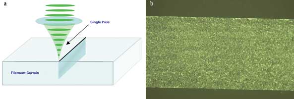
Figure 3. Filament cutting allows strengthened glass to be cut in a single pass as shown here (a) schematically; (b) shows magnified details of the high quality of the resulting cut edge. Courtesy of Innolas.
For example, 700-µm strengthened glass can be cut at up to 500 mm/s, leaving edges with a groundlike surface roughness of Ra = 2 µm and excellent bend strength. It also can produce tight curves to enable simultaneous processing of any holes and slots.
Filament cutting also can be used to cut sapphire for smartphone camera windows. Sapphire, which is even tougher than strengthened glass, must be cut with tight curves because the typical diameter of the window is about 5 mm.
Subnanosecond lasers for micromachining
While ultrafast lasers offer better processing results than nanosecond lasers, they also represent a significant cost increase over DPSS and fiber lasers. A completely new breed of Q-switched subnanosecond laser has been developed to service several applications that can benefit from slightly better results than achieved with traditional nanosecond lasers, but which cannot support the higher cost of switching to ultrafast lasers.
Traditional Q-switched micromachining lasers have pulse widths as long as tens of nanoseconds. There are numerous factors that determine the pulse width of a Q-switched laser. For example, the stimulated emission cross section of the laser crystal and the reflectivity of the cavity mirrors determine how many passes the light can make around the cavity before the gain is drained and the pulse dies away. But, ultimately, the pulse width is limited by the cavity length itself. Consider that light travels roughly 30 cm in 1 ns. So, even if the pulse makes just five round-trip passes, achieving a pulse width of 1 ns requires a cavity length of only 3 cm. If the pulse lasts for more passes, an even shorter cavity is required. (This significantly limits the minimum pulse width for fiber lasers.)
In the new Coherent Helios series DPSS lasers, engineers have miniaturized the cavity and its components, resulting in an effective cavity length of a few millimeters and pulse widths of between 400 and 600 ps. The near-IR output of this oscillator is a fairly modest 1 W at a repetition rate of 50 kHz because of the small gain crystal. A master oscillator power amplifier (MOPA) arrangement is used to boost the power for high-throughput applications. The use of modular and similarly miniaturized amplifier stages results in 2.5 W of output for models with one stage of amplification and 5 W of near-IR for models with two amplifier stages. This high peak power also supports very efficient but economical extracavity frequency doubling, enabling the recent release of a green (532 nm) model delivering pulse energies of 60 µJ at 50 kHz for an average power of 3 W.
A number of laser micromachining applications are now turning to these compact lasers because they match some of the advantages of ultrafast lasers but, in some cases, cost only a tenth as much. They are being used to dice thin semiconductor wafers as well as thin sapphire.
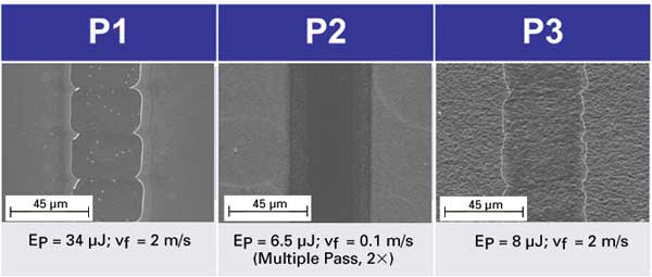
Figure 4. Examples of thin-film micromachining using a Coherent Helios 532-nm subnanosecond laser. The P1, P2 and P3 scribes are key steps in the fabrication of thin-film photovoltaics. Courtesy of Laser Zentrum Hannover.
Subnanosecond pulses are also useful for patterning thin films such as the transparent conductive oxides used in touch screens and the metals used in photovoltaics. Additionally, in some of these applications, the short pulse supports film removal by means of laser spallation of CIGS (Figure 4). Here, the laser ablates a relatively small total amount of material at the film/substrate interface, causing removal of all the overlaying layers. The result is rapid film patterning using only modest average laser power.
Meet the authors
Oliver Haupt is senior product manager at Coherent Inc. in Germany; email [email protected]. Dirk Müller is product line manager at Coherent Inc. Frank Gäbler is director of marketing for the material processing segment at Coherent Inc. in Bloomfield, Conn.