
Optical chip enables affordable holographic displays
When Daniel Smalley saw the Mark II holographic video display at MIT, he had to have one. And he will, thanks to a new approach he devised that could produce reasonably priced standard-definition, full-color holograms.
“I had to come up with something much, much less expensive,” Smalley, who recently defended his thesis at MIT Media Lab, told Photonics Spectra. “The Mark II was, and still is, a sprawling mass of expensive, one-of-a-kind electro-optics, originally run by a 6-ft rack of RF [radio frequency] electronics and a supercomputer.”
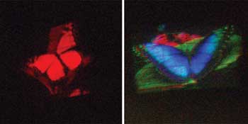
A hologram of a butterfly, displayed on both a conventional, monochromatic holographic-video monitor (left) and the MIT researchers’ new color monitor, which used an optical chip built by Daniel Smalley for roughly $10.
At the heart of his display is an optical chip resembling a microscope slide that Smalley built for about $10. It starts with a layer of silicon dioxide deposited by physical vapor deposition on a lithium niobate wafer.
“A layer of photoresist follows, which is patterned by photolithography, and then the wafer is immersed in hydrofluoric acid, which etches the exposed silicon dioxide and creates a ‘hard mask,’ ”
he said. After the resist is removed, the wafer is put in benzoic acid, which creates waveguides on parts of the surface not protected by silicon dioxide.
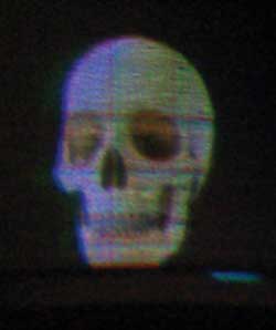
A photograph of a holographic stereogram created using anisotropic leaky-mode modulators and a frequency-division technique for color.
“The silicon dioxide is removed, leaving the bare wafer with proton-exchanged waveguides,” he said. “This becomes the substrate for a second patterning step in which resist is spun on and patterned photolithographically.”
After aluminum is deposited, the result is an aluminum interdigital transducer. RF signals exciting the transducer transfer some of this electrical energy to mechanical waves via the piezoelectric effect.
“These waves which travel along the wafer surface interact with light trapped in the waveguide,” Smalley said. “The light is mode-coupled out of the waveguide where it exits the far etch of the device to form a holographic image.”
Although they’ve been approached by “one or two manufacturers,” most consider the technology to be five to 10 years away from commercialization, he said.
Smalley has joined the electrical and computer engineering department at Brigham Young University, but will continue to collaborate with MIT on holographic video research, including fabricating new spatial light modulators and building new display geometries.
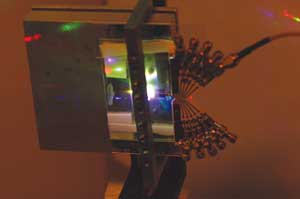
Anisotropic leaky-mode modulator for creating holographic video images.
The modulator is illuminated with red, green and blue laser light to
create a full-color hologram using a novel frequency-division technique.
Images courtesy of Daniel Smalley.
“The real contribution to our work has been the introduction of a new platform for holographic video research,” he said. “There is an enormous number of experiments to be done to fully explore this space.”
For now, Smalley is happy to report that “at long last, I am able to build the display I’d originally envisioned.”
The technique was detailed in Nature (doi: 10.1038/nature12217).
Published: September 2013