To take communications to the next level, laser technologies must improve in terms of cost, efficiency and robustness. Fortunately, those improvements are in the works.
Whether traveling through free space or over a fiber, lasers power data delivery – so laser innovations can up data rates, cut costs and improve capabilities.
Arguably, the greatest need for better communications lies in data centers, the conglomeration of computers and storage that make the online world go. Networking giant Cisco predicted in October 2013 that global data center traffic would triple between 2012 and 2017, reaching 7.7 billion terabytes annually. Three-quarters of the fastest-growing segment, cloud traffic, will take place within the data center itself, according to Cisco. Not surprisingly, dealing with this coming onslaught has attracted considerable interest. Few of the connections in data centers today are photonics-based, but that may change, with new types of lasers possibly playing a leading role.
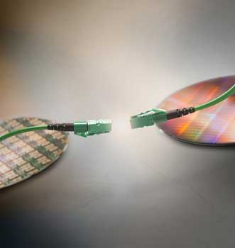
Data center optical communications will require low-cost connectors because as many as 1 million of them will be needed at one facility. Courtesy of Intel.
For instance, Intel is sampling silicon photonics products now and is preparing to ramp into volume manufacturing. “Our technology is based on the hybrid silicon laser,” said Mario Paniccia, an Intel fellow and general manager of the chip maker’s silicon photonics operations.
The Santa Clara, Calif.-based company’s approach marries light-emitting III-V compound semiconductors with silicon. The technology bonds bars of indium phosphide atop waveguides fabricated in silicon. When excited electrically, the InP produces light, which evanescently couples into the silicon waveguide. The compound semiconductor acts as an optical gain medium, and the result is a laser that can be used for communication.
The periodicity and depth of the gratings patterned in the waveguides
largely fix the wavelength of the laser, although electrical and other
techniques allow some tuning. The lasers operate at 1310 nm, which,
along with 1500 nm, is a standard telecom wavelength. Two benefits of
using these wavelengths: Silicon is transparent to IR, and such light
travels down fibers without loss.
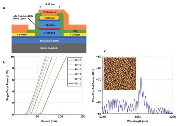 Indium arsenic quantum dots (b) act as the optical gain medium in a hybrid silicon laser (a) that can operate uncooled (c). Photo courtesy of Dr. John Bowers, University of California, Santa Barbara.
Typical runs in a data center are a few hundred to perhaps 1000 m, not the many kilometers of metro or long-haul telecom. The communication rates within data centers today are moving from 10 to 100 Gb/s, and in the future, on to 400 or 1000 Gb/s. An optically based communications solution is likely to first appear by multiplexing different laser channels of the same wavelength on separate parallel fibers. Thus, a 100-Gb link might initially be made up of four 25-Gb links. For cost reasons, eventually the multiplexing will be done using a scheme that puts lasers of different wavelengths down the same fiber.
To do wavelength multiplexing, however, sufficient laser performance in terms of holding a specific wavelength at some evenly spaced grid must be achieved. Also, the cost of the laser must drop to a point where the cost of the fiber and any coupling becomes dominant. In achieving cost reductions, Intel’s approach could offer an advantage.
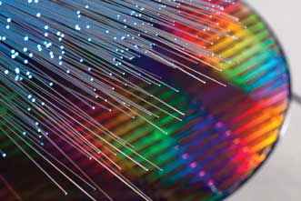
Optical fiber atop an Intel silicon photonics wafer, on which multiple parallel lasers can be built for the price of one.
“I can make one waveguide. I can make four. I can make eight. Or I can make 16. So, now I’ve made 16 lasers, essentially for the same price as one,” said Victor Krutul, director of marketing for Intel’s silicon photonics operations.
Raymond G. Beausoleil heads the large-scale integrated photonics research group at computer maker Hewlett-Packard Development Co. LP (HP) of Palo Alto, Calif. He is working on what will be needed in data centers five or even 10 years down the road. By then, light-based communications over fiber – instead of electrons traveling over copper – may be necessary, in part to meet power requirements. As data rates move up, pushing all those signals down a copper trace consumes more and more power. The problem is made more acute because it also ups the cooling load, adding to the overall power consumption.
However, the vision of light replacing electrons in data-center communications requires some substantial improvements in three laser parameters, Beausoleil said. The first is cost, with the laser for each channel needing to come in at substantially less than $1. The second: The devices must be energy-stingy, with something like 10 percent wall-plug efficiency. And the third is that they must be reliable and robust, since there may be a million or more of them in a data center.
All in all, these future lasers must be as much as 10 times better than current devices in those three areas. This also must be done for lasers multiplexed by wavelength.
Beausoleil is looking into using lasers made of hybrids of silicon and compound semiconductors. In this case, silicon microrings made using waveguides perhaps ¼ µm high and ½ µm wide form the basis for the lasing geometry.
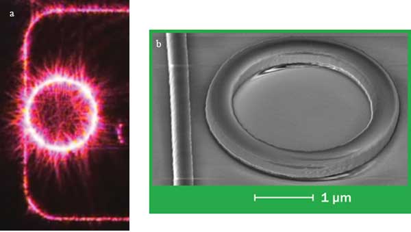
A microring (b) constructed using light-directing silicon waveguides (a) can form the basis for a hybrid silicon laser. Photo courtesy of HP.
Fabricating the silicon structures is not as easy as it seems because of the need to create output wavelengths that are spaced exactly 80 or 100 GHz apart. That places some tight constraints on the silicon feature dimensions.
“If you’re off by 10 to 15 nm, you find that, instead of being 80 GHz apart, two of your modes are 60 GHz apart,” Beausoleil said.
The microring variations from the ideal can be trimmed using electrical or thermal means, he added. The researchers have proved that this scheme works in the lab. They are now in the process of porting it to a large silicon wafer fab, where parameters may be tweaked to achieve cost, reliability or performance targets.
Aurrion Inc. of Santa Barbara, Calif., is another player in the same arena. The company has demonstrated an important capability in wavelength division multiplexing (WDM) of lasers, said Eric Hall, vice president of business development. “These are arrays of lasers on a WDM grid that keep that grid even as the ambient temperature changes. It allows you to maintain a high-bandwidth link in an uncooled environment.”
The company is working on both drop-in replacements for current copper connections and on connections for entirely new computer architectures. For the latter, one idea under discussion by the industry is computer-rack or even larger-scale integration. This takes advantage of the capability that photonics offers to separate modules and thereby optimize systems. Processors can be physically distant from other components, for example. This freedom to move things around can cut the costs of boards, make it easier to upgrade them and improve overall performance.
Aurrion was co-founded by Dr. John Bowers, a professor of nanotechnology at the University of California, Santa Barbara. He has worked with Intel and HP on hybrid silicon laser technology. Some of his latest research is on lasers created by combining silicon waveguides with quantum dots made of indium and arsenic. The III-V compound semiconductors in the InAs quantum dots provide the optical gain, while the silicon offers low cost and a very high performance platform. Devices built with the combination have a low threshold to initiate lasing and do so up to 120 °C, making uncooled operation possible. The method also offers another important performance-related capability.
“Alan Liu, the student at UCSB who grew the lasers, has now seen continuous-wave powers of over 170 mW from InAs quantum dot lasers on silicon,” Bowers said.
At California Institute of Technology in Pasadena, applied physics professor Dr. Amnon Yariv and his research group are working on a new semiconductor laser design, principally to address a looming issue: As more data is sent down a fiber, demands grow for greater temporal coherence of the source. Today’s commercially available lasers fall well short of what is needed, he said.
“In the short-to-medium range, we will need lasers with Schawlow-Townes linewidths of less than 10 kHz,” Yariv added. “Present commercial distributed-feedback semiconductor lasers possess, typically, between 0.5 and 1.0 MHz.”
Results from the first prototypes based on the new design are in the process of being published. They indicate positive progress toward the goal of greater coherence in laser output, he said.
It’s important to keep in mind that improvements are also needed in laser packaging, particularly with regard to cost, said Mitchell Fields, director of product strategy for the fiber optics division of San Jose, Calif.-based Avago Technologies. The company makes laser and receiver modules for all data communication distances, from the millimeters or meters inside a data center to the tens of kilometers for runs between cities or nations.
For long-haul and WDM applications, technology fundamentals and the operating environment tend to favor tightly sealed hermetic packaging, Fields said. In contrast, in a data center it’s possible to take advantage of packaging that is nonhermetic – particularly for vertical-cavity surface-emitting laser technology – and thereby hold down expenses, he added.
Even in such a controlled environment, however, packaging is a large component of cost – and that illustrates an important point to keep in mind about lasers and communications now and in the future, Fields said. “You can have a very cheap device, but in the end, the cost of the final module may be dominated by packaging and manufacturing technology, rather than the cost of the laser or receiver.”