Incandescent bulbs may be a thing of the past, but the principle of light-emitting filaments may have a new use in displays and optical communications.
Researchers from the U.S. and South Korea collaborated to develop an on-chip visible light source using filaments made of graphene. They attached small strips of graphene to metal electrodes, suspended the strips above a silicon substrate, and passed a current through the filaments to cause them to heat up and emit light.
"We've created what is essentially the world's thinnest light bulb," said Columbia University engineering professor James Hone. "This new type of broadband light emitter can be integrated into chips and will pave the way towards the realization of atomically thin, flexible and transparent displays, and graphene-based, on-chip optical communications."
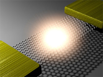
Schematic illustration of electrically biased suspended graphene and light emission from the center of the suspended graphene. Images courtesy of Young Duck Kim/Columbia Engineering.
The ability to create light in small structures on the surface of a microchip is a crucial step towards the development of fully integrated photonic circuits. Researchers have developed many approaches to do so, but have not yet been able to put the oldest, simplest artificial light source – the incandescent light bulb – onto a chip.
This is primarily because light bulb filaments must be extremely hot – thousands of degrees Celsius – in order to glow in the visible range, and microscale metal wires cannot withstand such temperatures. In addition, heat transfer from the hot filament to its surroundings is extremely efficient at the microscale, making such structures impractical and leading to damage of the surrounding chip.
The ability of graphene to achieve such high temperatures without melting the substrate or the metal electrodes is due to another interesting property: as it heats up, graphene becomes a much poorer conductor of heat. High temperatures are confined to a small “hot spot” in the center.
"At the highest temperatures, the electron temperature is much higher than that of acoustic vibrational modes of the graphene lattice, so that less energy is needed to attain temperatures needed for visible light emission," said Myung-Ho Bae, a senior researcher at the Korea Research Institute of Standards and Science (KRISS). "These unique thermal properties allow us to heat the suspended graphene to up to half of the temperature of the sun and improve efficiency 1000 times, as compared to graphene on a solid substrate."
By measuring the spectrum of the light emitted from the graphene, the team was able to show that graphene was reaching temperatures of above 2500 °Celsius, hot enough to glow brightly.

"The visible light from atomically thin graphene is so intense that it is visible even to the naked eye, without any additional magnification," said Young Duck Kim, a postdoctoral research scientist at Columbia.
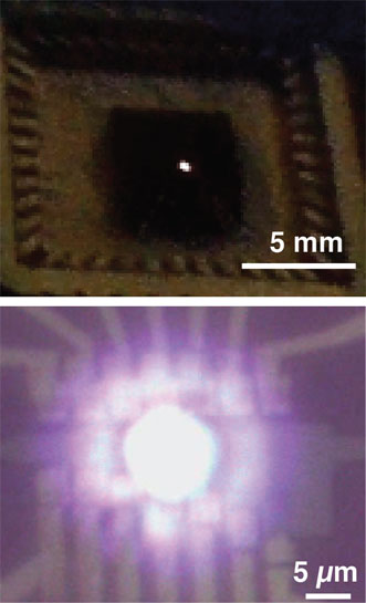
An optical image, top, and micrograph, bottom, of bright, visible light emission from suspended graphene.
The spectrum of the emitted light showed peaks at specific wavelengths, which the team discovered was due to interference between the light emitted directly from the graphene and light reflecting off the silicon substrate and passing back through the graphene.
"This is only possible because graphene is transparent, unlike any conventional filament, and allows us to tune the emission spectrum by changing the distance to the substrate," Kim said.
The team also demonstrated the scalability of their technique by realizing large-scale arrays of graphene light emitters grown with a chemical vapor deposition (CVD) process.
"Edison originally used carbon as a filament for his light bulb, and here we are going back to the same element but using it in its pure form – graphene – and at its ultimate size limit – one atom thick," said Yun Daniel Park, professor in the department of physics and astronomy at Seoul National University.
The group is now working to further characterize the performance of these devices – for example, how fast they can be turned on and off to create bits for optical communications – and to develop techniques for integrating them into flexible substrates.
"We are just starting to dream about other uses for these structures – for example, as micro hotplates that can be heated to thousands of degrees in a fraction of a second to study high-temperature chemical reactions or catalysis," Hone said.
U.S. funding came from the National Science Foundation, Air Force Office of Scientific Research, Office of Naval Research, Army Research Office and Qualcomm Innovation Fellowship. Korean funding came from the National Research Foundation, Center for Advanced Soft Electronics through the Global Frontier Research Program, Priority Research Center Program, Center for Topological Matters at the Pohang University of Science and Technology (POSTECH).
The research was published in Nature Nanotechnology (doi: 10.1038/nnano.2015.118).
For more information, visit engineering.columbia.edu.