SOUTHAMPTON, England, July 13, 2015 — A new chemical vapor deposition process allows fabrication of wafer-scale films of molybdenum disulfide (MoS2), which until now has been commercially available only in microscale flakes.
The advance could pave the way for the large-scale manufacture of flexible and transparent optoelectronics, gas sensors, memory devices, and photovoltaics.
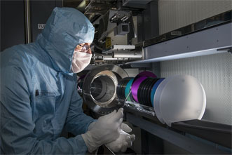
Researchers at the University of Southampton's Zepler Institute used room-temperature, ambient-pressure chemical vapor deposition to create the ultrathin films.
A new chemical vapor deposition technique allows creation of wafer-scale MoS2 films at room temperature. Courtesy of the University of Southampton.
Working at room temperature — rather than at the 800 to 900 °C temperatures typically used — makes it possible to deposit MoS2 on a range of substrates, namely those with low thermal stability, such as flexible displays. The technique also minimizes stress on other previously deposited layers and helps reduce processing costs.
MoS2 has exceptional charge carrier mobility and is widely believed to be a strong contender for the next generation of electronics, as the silicon chip reaches its fundamental limits. In addition, MoS2 is an N-type semiconductor, useful for photovoltaics.
"There have been extraordinary efforts devoted to the study of 2D materials, especially MoS2," said professor Shen Ze Xiang of Nanyang Technological University in Singapore, which is affiliated with Southampton. "For these materials to be useful in real applications and for many fundamental studies, the ability to fabricate uniform, large-area thin films is critical."
Xiang said the new deposition technique has allowed Nanyang researchers to study ultrafast carrier thermalization and cooling dynamics in few-layer MoS2.
The work was carried out under the Chalcogenide Advanced Manufacturing Partnership (ChAMP), funded by the U.K. Engineering and Physical Sciences Research Council.
For more information, visit http://chalcogenide.net.
