DRESDEN, Germany, May 16, 2016 — Achieving both miniaturization and high resolution in organic light-emitting diode (OLED) displays has been a challenge, as conventional materials processing methods such as photolithography cannot easily be applied to organic semiconductor materials. Now electronic beam (e-beam) technology has been used to create micropatterns in the emission area of OLEDs, a process that could enable high-pixel-density microdisplays for augmented/virutal reality systems and other mobile displays.
Because the e-beam process takes place after the OLED is encapsulated, it is possible to build a highly productive OLED before the e-beam is used to modify the emission. The energy of the electrons determines their penetration depth in the OLED’s layer stack. By selecting the appropriate process parameters, the encapsulation can also be penetrated by the e-beam; and the luminous characteristics of the organic layers beneath can be patterned without destroying or compromising the encapsulation itself. In some applications it is possible to modify the individual layers of the OLED directly.
 Researchers at the Fraunhofer Institute for Organic Electronics, Electron Beam and Plasma Technology (FEP) demonstrated this approach by using an e-beam to structure an image of the Dresden Semperoper in 100 seconds. Even with a write time of less than two minutes, an impressive resolution of 12,700 dpi was attained, corresponding to 2μm spacing of the image dots. The researchers structured the OLED using an e-beam lithography system from Raith GmbH.
Using the white OLED shown below, the image of the Dresden Semperoper was structured with the electron beam in 100 s. Courtesy of Fraunhofer FEP/Fotograf Semperoper: Christof Lippmann.
“Continuous gray scales in an image can be created on a monochrome OLED using the electron beam, while at the same time the local current consumption is reduced,” said Elisabeth Bodenstein, a member of the research & development team. “The longer the dwell time on one spot with the beam, the darker the OLED will appear there.”
The e-beam technology can be adapted for use with different OLEDS, including OLEDs that are applied to a rigid medium or a flexible film. It can be used regardless of the OLED’s color or whether the substrate is optically opaque, translucent or transparent. The size of the substrate is universal and can be matched to the corresponding application.
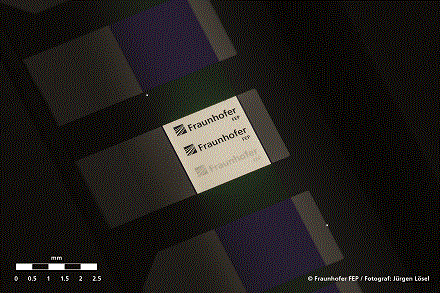
White e-beam micropatterned OLED. Courtesy of Fraunhofer FEP /Jürgen Lösel.
The research team is planning to enhance the e-beam technology to allow full-color patterning and is preparing to work with industrial partners to apply the e-beam technology. The technology was developed within a project funded by the Fraunhofer Gesellschaft.
The FEP will present micro-OLEDs patterned using e-beam technology during SID Display Week 2016, May 24-26, in San Francisco.