JOSE POZO, EUROPEAN PHOTONICS INDUSTRY CONSORTIUM (EPIC)
Less than a year after the development stage launch of three photonic pilot lines funded by the European Commission, one of these lines is set to provide open industry access to novel spectrometers operating in the mid-IR range: MIRPHAB (Mid-infrared photonics devices fabrication for chemical sensing and spectroscopic applications).
Chemical sensors are everywhere, playing an important role in increasing the quality of life. They assess air and water, and monitor food. In medical diagnostics, inline chemical sensors will soon enable efficient breath analysis along with the rapid and continuous analysis of body fluids. Furthermore, they are critical in industrial process control, analyzing the composition of samples in the petrochemical, pharmaceutical and automotive industries.
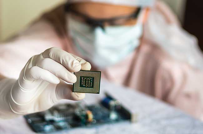
The smart assembly of the building blocks in MIRPHAB follows strict rules, making it suitable for volume manufacturing. Courtesy of EPIC, source Shutterstock.
Yet in all of these applications, industry has a clear unmet need: cost-effective sensors that operate on a real-time basis and can easily integrate into existing equipment, or for online or even in-situ monitoring. These requirements offer an opportunity for spectroscopy, which in essence examines the alterations in the spectrum of light when interacting with matter — in gas, liquid or solid form. Applications include monitoring vehicle emissions, assessing drinking water, or performing quality control of pharmaceuticals. No matter what the form, material absorbs certain regions of the spectrum or wavelength range depending on its composition.
The mid-infrared (MIR) region is already the favored wavelength band, with applications that include chemical emission monitoring, process control, high-sensitivity trace detection and biological-sensing applications. The best way to get precise and reliable information is to rely on spectroscopic analyses and, among the technologies now available, tunable diode laser absorption spectroscopy (TDLAS), which uses a tunable laser to sweep over certain wavelengths. This allows for the unambiguous detection of chemicals. Semiconductor-based solutions employ tunable semiconductor laser sources and photonic integrated circuits are the answer for compact, cost-effective and low-power consumption sensors. The MIRPHAB pilot line aims to supply this industrial need by providing the first prototypes with a fabrication process scalable to volume production.
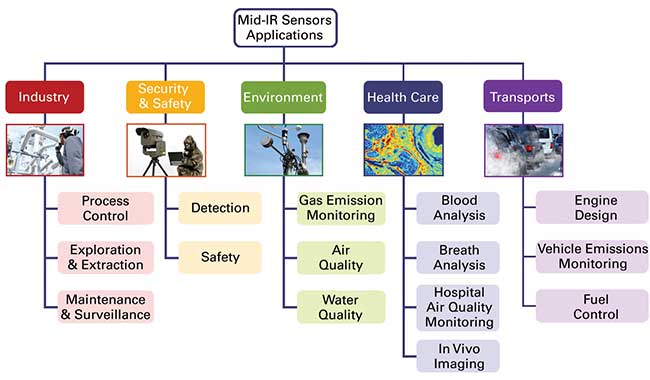
Applications of mid-infrared spectroscopy. Courtesy of TEMATYS.
Miniaturization and affordability
The current market of chemical detection is dominated by gas chromatography (GC), which involves chemical analytics that separate chemicals in a complex sample, and Fourier transform infrared spectroscopy (FTIR). It’s a similar technique to TDLAS, but uses a broadband source and simultaneously collects high spectral resolution data over a wide spectral range. FTIR and gas chromatography together represent a $2 billion-per-year market with a compound annual growth rate above 4 percent in the last few years. There are, however, some major drawbacks for GC and FTIR instruments. In GC, the cost of the installations and the complexity of the measurement require highly trained personnel, representing a barrier to a widespread use in online or inline analyses. Furthermore, the typical size of the tools and the need for specific installations substantially prevent their use in portable applications.
The second notable limitation comes from the use of a high-purity carrier gas acting as the mobile phase during the measurement cycle. For FTIR instruments, one major drawback comes from the optical interferometers containing moveable mechanical parts that must always be aligned with high precision. The other drawback is that since a broadband light source is used, it is difficult and expensive to illuminate with high brightness at any particular wavelength.
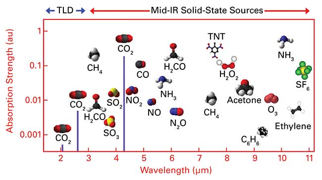
Figure 1. Chemical compounds that can be detected in the mid-infrared wavelength region. Courtesy of CEA-LETI.
Fingerprint wavelength
Laser-based MIR absorption spectroscopy in the so-called fingerprint wavelength band (3 to 12 μm) has been proven to allow unambiguous identification of substances (Figure 1), providing real-time detection of trace chemicals; it’s the best potential solution for overcoming the limitations of GC and FTIR. But in order to use TDLAS in the MIR region, novel lasers that can be tunable to specific wavelengths are needed. There are two types of solid-state laser sources with such capability: intraband cascade lasers (ICLs) and quantum cascade lasers (QCLs). Using ICLs and QCLs as high-brightness and precise spectroscopic light sources offers outstanding advantages. The high spectral brightness of ICLs and QCLs support, on one hand, fast detection in gaseous, liquid or solid phase, and, on the other hand, a strong miniaturization of the devices.
However, ICLs and QCLs are less mature than the light sources typically used in FTIR, and have a broad tuning range, small footprint and low power consumption at the research stage (Figure 2). From a commercial standpoint the wavelength coverage is still limited and, when multi-components have to be measured, MIR-TDLAS cannot yet compete against GC and FTIR.
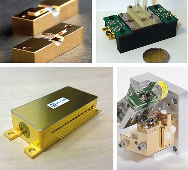
Figure 2. (Top, left) Quantum cascade lasers (QCL) placed on a sub-mount for testing purposes. (Top, right) Miniaturized photo-acoustic sensor. (Bottom, left) Assembled and professionally packaged MIR sensing module. (Bottom-right) Integration of a QCL with scanning MEMS grating as wavelength-selective feedback element (footprint 50 × 40 mm2). Courtesy of MIRIFISENS project.
The MIRPHAB pilot line was launched Jan. 1 to facilitate the acquisition of prototype spectrometers based on MIR-TDLAS. Its mission was two-fold: (1) to fabricate prototypes in such a way as to address the production volumes that the market demands, and (2) to provide those prototypes to industry. The second part of the mission has now begun.
Smart assembly of building blocks
MIRPHAB’s mission is to provide assembled modules based on components and building blocks for laser-based optical spectroscopic sensors. Such building blocks can be selected from an extended list of wavelength-tunable MIR light sources including ICLs and QCLs, photodetectors, integrated measurement cells and integrated MIR photonic chips. The full current list can be found at www.MIRPHAB.eu, and it is expanded as the pilot line evolves during its development phase until 2020. These building blocks are provided by leading European industrial suppliers of MIR photonic components, complemented by a network of first-class European research institutions with well-equipped semiconductor processing clean rooms, capable of carrying out pilot line production. Figure 3 shows the technologies covered by MIRPHAB by categories and spectral coverage, indicating also the wavelength range within the MIR spectrum covered by a certain component or device. These devices are based on merged III-V and Si-based technologies, combining mid-IR lasers such as QCLs and ICLs, silicon photonics and MEMS devices, critical to the realization of the novel generation of miniaturized devices with superior performance.
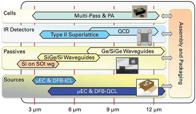
Figure 3. Technologies provided by MIRPHAB pilot line covering the wavelength range of 3 to 12 µm. Courtesy of the MIRPHAB project.
The MIRPHAB building blocks can be grouped in four families. The smart assembly of one or several building blocks of each of these families will result in a spectrometer satisfying the needs of the customer:
Light sources:
Specifically with respect to wavelength-tunable MIR laser sources (QCL and ICL), MIRPHAB builds on the technological results achieved within a series of previous and current publicly funded R&D projects, including the EU-funded MIRIFISENS, Clarity, Doggies, ICSpec, WIDELASE and CHEQUERS. The mature laser sources resulting from this technology transfer are provided by the European companies Alpes Laser, Nanoplus and MirSense, together with the Fraunhofer institutes IAF, IPMS and IPT. If novel epitaxy is needed, the capabilities of IQE and Compound Semiconductor Technologies (the global leaders in the design and manufacture of advanced semiconductor wafer products) can also be used.
Detectors:
Regarding MIR photodetectors, already commercially available cadmium mercury telluride (CMT) variants are complemented by cadmium and mercury-free III-V compound semiconductor-based MIR detectors, offering an improved long-term stability and routes to integration on silicon-based technology platforms. In addition, while cryogenically cooled III-V type II super lattice (T2SL) detectors are mature, based on the same technology, room-temperature or just thermo electric (TE)-cooled detector variants will be derived during the development phase and are complemented with InAsSb-based detectors and quantum-cascade detectors (QCD). Such detectors are provided by the European companies III-V labs and Vigo System S.A.
MIR micro-optics and photonic integrated circuits (PIC):
MIRPHAB provides micro-optic and integrated-optic components and modules for MIR photonics. For MIR PIC and integrated sensor solutions, MIRPHAB again relies on the outstanding technological results achieved within the R&D projects mentioned above, where the feasibility of a wideband MIR photonics based on Si and Ge materials has been demonstrated. Such PIC waveguide platforms are silicon on insulator (SOI) for wavelengths between 2 and 4.5 µm, SiGe on Si for wavelengths between 3.5 and 7.4 µm, and Ge on SiGe for wavelengths between 7.4 and 11 µm. The optical circuitry is provided by the European institutes CEA-LETI, CSEM and IMEC, while instructions for their design and even training for designers are provided by the European company PhoeniX Software.
Assembly and packaging solutions and reliability tests:
According to the specifications provided by the users, the building blocks will be chained together either by hybrid or monolithic assembly and combined with MEMS and electronics to realize systems-in-package or systems-on-chip devices with extended functionalities. Also, depending on such user-driven specifications, targeted reliability studies can be implemented. The packaging, engineering and reliability studies are supplied by the institutes CSEM and CEA-LETI.
From chemical sensing to industry
These MIR spectrometers represent the next generation of sensors that are compact, inexpensive, low on power consumption and capable of real-time detection where the speed and sensibility is unrivaled. The wavelength region targeted (3 to 12 μm) is crucial for many applications, including materials processing, chemical and biomolecular sensing, security and industry. The enabled volumes and, consequently, cost reduction will enable application in a vast number of new fields. For instance, these devices are expected to improve the quality of daily life by providing continuous monitoring of emissions resulting in more stringent environmental regulations pushing for reliable, cost-efficient and accurate solutions. In addition, MIR spectrometers enable both atmospheric and public-access building air monitoring. In the field of water-quality monitoring they can enable analyzers in automated warning stations to provide real-time information about the quality of water.
In security and safety, the detection of drugs and explosives remains an enormous societal challenge that must be addressed by protecting transport systems detecting explosives, weapons and illegal items. MIR sensors can scan from a distance of up to 30 m and are capable of instantaneous, real-time, unambiguous detection. In particular, customs and border protection requires rapid and automated detection, whether the threat is inside a vehicle or the middle of a shipment. Furthermore, automated detection systems are required for standoff hazardous gas detection, radionuclide monitoring, or fire detection in power plants, embassies, high-risk facilities, transportation and government agencies.
In health care, the dream of noninvasive blood analysis could be even closer, with target monitoring of, for instance, glucose, hemoglobin and oxygen-saturation levels. Furthermore, the detection of certain molecules can be an indicator for the rapid and early detection of infections.
Financing for early adopters
Companies with business in the aforementioned fields, or even others, can join the MIRPHAB community and benefit as an early adopter by gaining an upper hand on their competition. While the full pilot line will not be commercially available until 2020, as early adopters, European companies can receive co-financing of up to €230,000, or up to 70 percent of the manufacturing costs. This funding is supposed to compensate for the risk taken by early adopters for entering a pilot line in development, whose technology will not be mature until 2020. Those risks will be studied case by case, and clearly specified in the contract between the early adopter and the pilot line.
To access MIRPHAB prototyping services, companies should initiate the application process by registering directly at www.MIRPHAB.eu, which will give them access to a newsletter specifying deadlines for calls for application for open access, as well as up-to-date information on the new building blocks available. Once registered, companies can submit applications via the website. While access to MIRPHAB is open to all European and non-European companies, only European companies can request the co-financing grant.
Meet the author
Jose Pozo is director of technology and innovation at EPIC (European Photonics Industry Consortium). He has 15 years’ background in photonics technology, market knowledge, and a large network within the industrial and academic photonics landscape. Jose is a member of the board of the IEEE Photonics Society Benelux. He holds a Ph.D. in electrical engineering from the University of Bristol in United Kingdom and a M.Sc. and B.Eng. in telecom engineering.
Acknowledgments
EPIC wishes to thank the members of EPIC who constantly share their vision and ambitions; in particular, we would like to thank the partners of the MIRPHAB Pilot Line: CEA-LETI, Alpes Laser, Nanoplus, MirSense, the Fraunhofer institutes IAF, IPMS and IPT, III-V Lab, Vigo System, PhoeniX Software, CSEM, IMEC, TEMATYS, IQE, Compound Semiconductor Technologies, Bosch, Cascade Technologies, Quantared and Norsk Elektro Optikk.
MIRPHAB (mid-infrared photonics devices fabrication for chemical sensing and spectroscopic applications), is an EC funded project, with reference 688265, in a public-private partnership with Photonics21 (www.photonics21.com), with the ambitious goal of creating a commercially viable pilot line for the fabrication of mid-IR sensors that is ready for business by 2020. This result will be achieved by setting up and operating a fabrication platform with open access for fast mid-IR device prototyping to European industry. EPIC is in charge of the dissemination of the MIRPHAB project.