DIRK MÜLLER, COHERENT INC.
In manufacturing of semiconductor microelectronics, displays, medical devices and many other industries, there is an increasing trend toward higher-precision processing. This means cutting, drilling and marking parts with smaller feature sizes and greater accuracy, superior edge quality and with a reduced effect on surrounding material. In the past, most precision laser-based processing applications relied on nanosecond pulse widths or ultraviolet output (or both). But traditional sources cannot always service this new, demanding class of applications. As a result, some applications are now turning to lasers with ultrafast — picosecond or femtosecond — regime pulse widths to accomplish these tasks.
Ultrafast processing benefits
The goal of micromachining is the creation of micron-scale features, such as holes, grooves and marks, with high-dimensional accuracy while avoiding peripheral thermal damage to surrounding material. In other words, precise, clean cuts and marks with high surface quality and minimal heat-affected zone (HAZ).
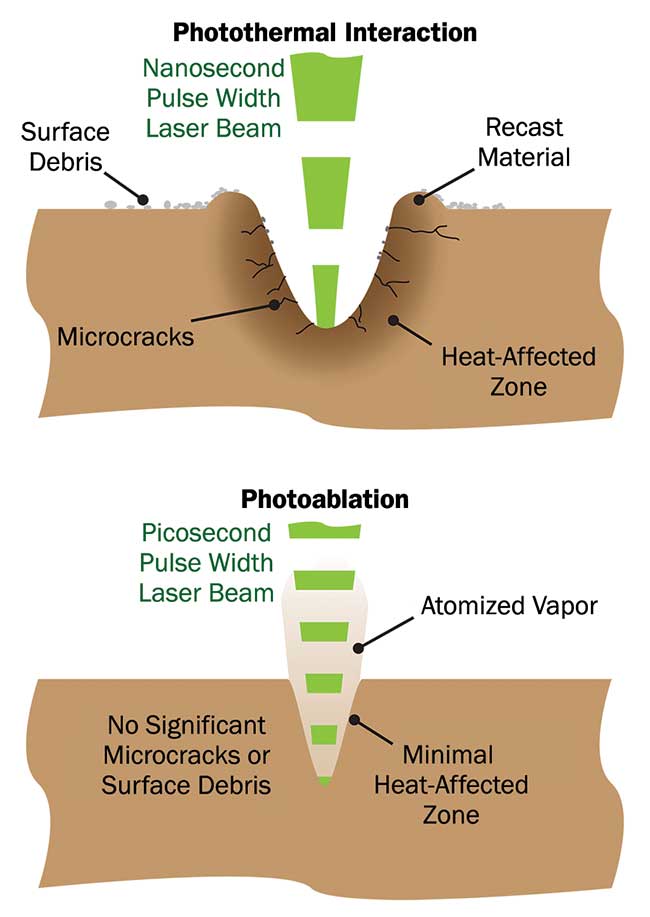
Schematic illustrating the major differences between ultrafast processing and processing with longer pulse width lasers. Courtesy of
Coherent.
There are two basic mechanisms by which a laser can precision drill, scribe, cut or mark a material. Many traditional applications rely on infrared and visible Q-switched lasers, which have pulse widths in the tens of nanoseconds range, and which remove material via a photothermal interaction. Here, the focused laser beam acts as a spatially confined, intense heat source. Targeted material is heated rapidly, eventually causing it to be vaporized — essentially boiled away.
The advantage of this approach is that it enables rapid removal of relatively large amounts of target material. Furthermore, nanosecond laser technology is mature; these sources are highly reliable and have attractive cost of ownership characteristics. However, for the most demanding tasks, peripheral HAZ damage and/or the presence of some recast material can present a limitation. This includes the delamination of surface coatings, microcracking, or changes in the bulk material properties.
One way of minimizing the size of the HAZ is to employ a nanosecond laser having output in the UV, rather than in the visible or near infrared. UV light is strongly absorbed by most materials, limiting how far the laser light penetrates into the part and therefore reducing the HAZ.
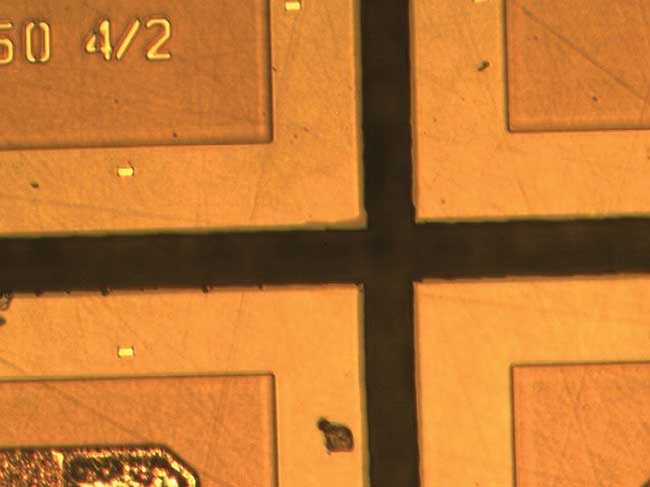
Results of stealth dicing a silicon carbide wafer with a picosecond laser, before mechanical separation of the individual dies. Courtesy of Suzhou Delphi Laser Co.
The second mechanism for laser material removal is based on photoablation, which involves directly breaking the molecular or atomic bonds that hold the material together rather than simply heating it. This can be performed with ultrafast lasers because their short pulsewidths lead to very high peak powers (megawatts and above). These high peak fluences drive multiphoton absorption, which strips electrons from the material and then explodes away because of Coulomb repulsion. When using ultrafast pulses, the material is exposed to the laser energy for such a short time that the energy can’t be carried beyond the area of impact, so the surrounding area stays cold. Energy left over after the bond-breaking process is carried away with the expelled particles. Together, these effects result in an inherently colder process with significantly reduced HAZ. This is also a very clean process, leaving no recast material and thereby eliminating the need for elaborate post-processing.
Another major advantage of ultrafast processing is that it is compatible with a very broad range of materials, including several high-bandgap materials including glass, sapphire and certain fluorinated polymers that have low linear optical absorption and are therefore difficult to machine with existing commercially available lasers. More specifically, the technique is “wavelength neutral”; that is, nonlinear absorption induces a light-matter interaction even if the material is normally transparent at the laser wavelength.
One limitation of ultrafast processing is that it provides lower material removal rates, and ultrafast lasers have been more costly than long pulse laser sources. As a result, ultrafast processing is typically reserved for applications that demand the greatest possible precision, quality and smallest HAZ.
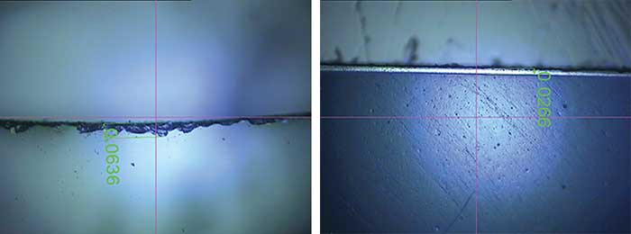
Cross sections of glass cut with a nanosecond laser (left) and a picosecond laser (right). The picosecond laser produced a cut with fewer microcracks and less residual debris. Courtesy of Suzhou Delphi Laser Co.
From sapphire cutting to LED dicing
Because of their advantages, ultrafast processing lasers have now been adopted in a number of demanding, high-precision applications. These include LED dicing; sapphire cutting; drilling of automobile engine fuel injection nozzles and engine cooling plates; hole drilling and structuring of biomedical filters; cutting and drilling of FR-4 resin; cutting and drilling of both low-temperature co-fired ceramics and high-temperature co-fired ceramics; and microprocessing of metals such as stainless steel and copper. More recently, picosecond lasers have also been used to mark integrated circuit packages. The short pulses ameliorate potential damage to the embedded die during marking.
Several Asian tool manufacturers have been using Coherent RAPID series picosecond lasers for several years now, specifically for semiconductor wafer dicing and glass cutting. Joshua Zhao, sales manager at Suzhou Delphi Laser Co. for the Americas region, discussed how the lasers are employed and the benefits they have delivered. “Wafer dicing can actually be accomplished in two different ways. In the first, called laser grooving, the beam is focused onto the surface of the wafer in the street area (the empty area between circuit components),” he said. “The laser makes a scribe part way through the wafer, and the individual chips are subsequently singulated mechanically. The second method is called stealth dicing. Here the beam is focused within the wafer itself, where it creates a scribe within the material. Again, the individual chips are then singulated mechanically, typically by tape expansion.
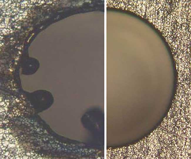
Comparison of a 200-µm-diameter hole drilled in stainless steel with a nanosecond laser (left) and a picosecond laser (right). The picosecond laser produced a cleaner hole with less recast material and a smaller heat-affected zone (HAZ). Courtesy of Coherent.
“Previously, we employed a 355-nm nanosecond laser for laser grooving, but now we’ve switched to a 1064-nm picosecond laser and perform stealth dicing. This has delivered several benefits. First, the picosecond laser produces a much smaller heat-affected zone than the nanosecond laser,” Zhao explained. “This allows the cutting street to be reduced in size from 25 µm, down to 14 µm. Which, in turn, results in a higher yield — that is, one can pack more devices onto a given wafer. Also, we have fewer pieces that don’t separate properly than before, generating less waste. As a result, we’re also able to run the process faster than before. For example, the nanosecond laser could process 15 wafers per hour, for a 10 mil × 23 mil chip size, but the picosecond laser can process 23 wafers per hour. Plus, we can even process thicker wafers; now we can dice 200-µm thick wafers, while our nanosecond laser process couldn’t go above 100 µm thickness.”
Picosecond laser glass cutting: avoiding cracks and debris
Another important picosecond processing application is glass cutting. This application is driven by the tremendous market growth for cellphones and tablet computers that incorporate touchscreens. There are two important trends in touchscreen display glass scribing. The first is a drive toward the use of thinner glass substrates in order to minimize the total weight of the display. The second is a need to cut curved shapes in the glass, rather than simply straight lines, in order to allow rounded edges on the display, as well as to accommodate more complex screen geometries.
As the display glass gets thinner, it is critical that the finished product still retain the ability to withstand being dropped, handled roughly and pressed upon (for touchscreens). A typical LCD touchscreen actually contains three or four stacked layers of glass. The topmost (outer) sheet is often a 700-µm-thick protective cover glass. To minimize the risk of scratching and breakage, this outer layer of the topmost glass is chemically treated to produce a very tough surface — Corning’s Gorilla Glass, Asahi’s Dragontrail and Schott’s Xensation are examples of this. The thickness of this strengthened layer typically runs tens of microns deep.
Traditional mechanical glass cutting can lead to microcracks and debris. Laser glass cutting, based on CO2 and nanosecond solid-state lasers, has been in use for some time in the display industry. Both of these lasers produce dramatically better results than mechanical cutting, but can each have some limitations, especially for very thin glass (<300 µm thickness). Zhao said, “[Picosecond laser cutting] yields a finished piece that has greater edge strength, and is much more resistant to breaking during use.”
A new generation of reliable, high-power, industrial ultrafast lasers is enabling higher-precision microprocessing in a variety of applications. Expect this technology to impact industries as diverse as microelectronics fabrication, medical device manufacturing and automotive production.
Meet the author
Dirk Müller, Ph.D., is the director of Strategic Marketing at Coherent, Inc.; email: [email protected].