DAVE KELLY AND ANDRES TAMEZ, COHERIX INC.
Automotive designers are more frequently turning to structural adhesives as a solution for strengthening, structurally optimizing and lightweighting automotive bodies. These adhesives enable mixing material types to achieve lightweight structures while meeting goals for safety, noise, vibration and harshness. Vehicle assemblies may now contain hundreds of adhesive beads. The dramatic increase in dispensed meters of these beads is driving a need for cost-effective, real-time, 100 percent 3D bead inspection. The inspection objective is to speedily and accurately detect and locate gaps and volumetric defects in the adhesive bead to support efficient in-process repair or rejection of defective beads.
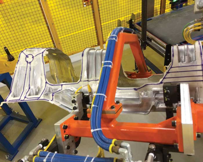
Vehicles may contain hundreds of adhesive beads. Those shown here in blue are on an underbody part. Courtesy of Coherix.
The bead inspection challenge was presented by the supplier of adhesive-dispensing systems who desired a self-contained 3D smart sensor that would reside at the dispensing nozzle. At high speeds and in real time, the sensor needed to be capable of 3D measurement of the bead — height, width and volume — at the point of dispensing. The focus application was automotive body-in-white sheet metal assembly where increasingly structural adhesive is replacing welding and riveting.
Demand for adhesive bead inspection has been growing for years. But existing solutions all have been 2D and deemed inadequate because of limited inspection capability (no bead height), large computer racks that are difficult to integrate and sensor sensitivity to environmental lighting.
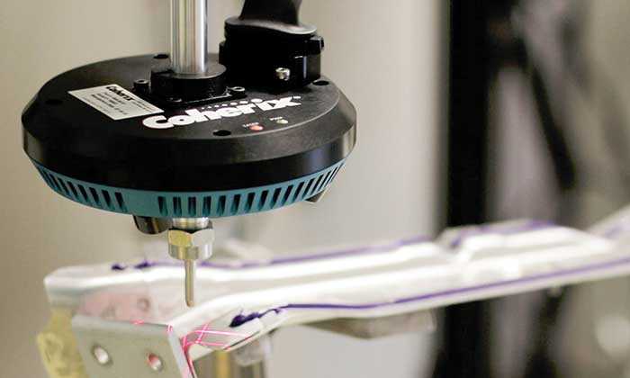
This 3D bead inspection sensor measures bead height, width and volume at high speeds and in real time. Courtesy of Coherix.
Basic 3D imaging of the bead as it is dispensed on the part can be accomplished by a number of well-known techniques. The technique chosen here, arguably the most robust, is laser line triangulation. As with most automation inspection applications, there are many layers of complexity to a complete and robust solution. The adhesive bead can be dispensed in any direction relative to the nozzle. The part can take any shape or form. The nozzle can be positioned obliquely to the surface. And the speed of the dispensing motion may vary.
A sensor residing on the nozzle capturing laser profiles either will need to track the bead mechanically or to surround the nozzle with 360-degree profile data. In either case, substantial information is required to process the profiles into a continuous and accurate bead path and location in 3D space. The 3D path and location is derived from a combination of a priori setup information recorded during system teach, speed and position information from the motion controller, as well as information derived from the part surface by the precalibrated laser profiles themselves. All of these data sources are handled by sophisticated algorithms and application software.
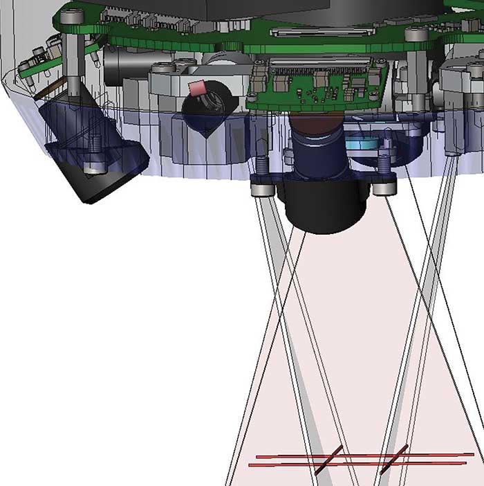
The solution described here enables continuous capture of surface profile data by surrounding the dispenser nozzle with four orthogonal, overlapping laser line profilers. From a systems design perspective, continuously measuring 360 degrees around the nozzle offers many advantages. These include capturing the part surface geometry prior- and post-bead dispense, completely mapping the nozzle orientation and distance relative to the surface, and avoiding the liability of mechanical motion.
The inspection sensor’s components are packaged into a compact optoelectromechanical design. Courtesy of Coherix.
The optoelectromechanical design requires an embedded vision architecture to integrate high-performance CPU capability for high-speed image capture, 3D processing, visualization and factory interfacing. Fortunately, such embedded vision architectures are becoming more common in high-end machine vision applications because of the availability of off-the-shelf CMOS image sensors, lasers, optics, advanced FPGAs and compact form factor single board computers or system on modules (SoMs). Additionally, the abundance of reference design IP and robust CAD/CAE tools accelerates design work and lowers the barriers of what used to be only the realm of camera specialists.
Design tools
Embedded vision systems span a diverse set of technologies and associated CAD/CAE design automation tools for both hardware and embedded code development. A core set of powerful but accessible tools, vendor IP blocks, reference designs and evaluation kits enable rapid and robust development. In addition, online user forums incubate an environment where engineers can quickly come up to speed on the tools and leading design techniques.
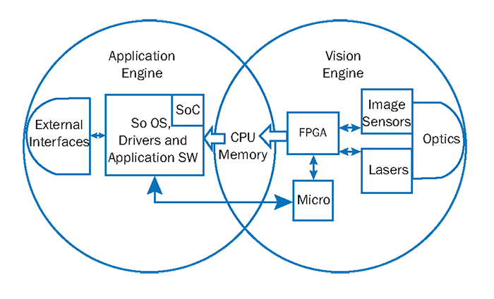
Within embedded vision architecture, the CPU memory bridges the vision engine and the application engine. SoC: system on chip. SoM: system on module. Courtesy of Coherix.
This project design workflow used three core tools to manage electrical, mechanical and optical compatibility and design optimization: Altium Designer for circuit board schematic design and layout; SOLIDWORKS for 3D mechanical and thermal design; and Zemax for optical design of field of view, focus depth, pixel resolution, illumination geometry and signal-to-noise ratio (SNR) modeling. Altium generates 3D STEP models and interfaces nicely with SOLIDWORKS, and Zemax outputs optical geometry to SOLIDWORKS. In addition, 3D printing was leveraged throughout the design process to build testable prototypes and achieve a compact but robust and assembly-friendly design.
For embedded logic, timing and control code development, the tools were dictated by the selected components — Xilinx FPGA and Microchip PIC32 microcontroller. The design workflow included three core tools: Xilinx Vivado Design Suite, ModelSim simulator, and MPLAB Integrated Development Environment and In-Circuit Emulator. These tools can be quickly accessed via evaluation kits or development boards that include example projects and libraries that can be retargeted to the specific embedded design.
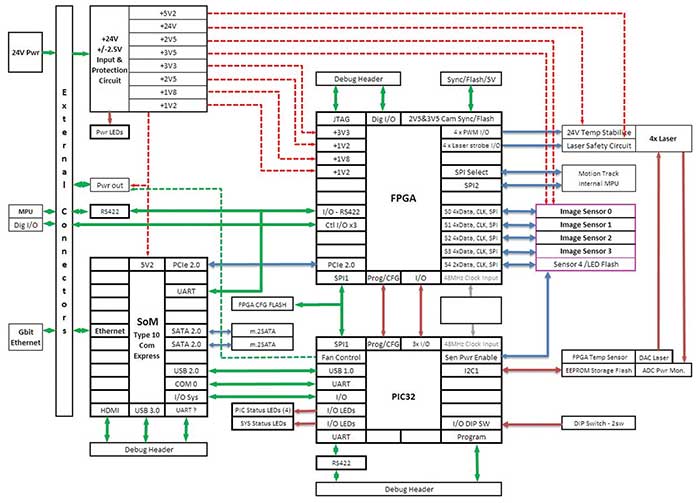
The embedded design integrating FPGA, PIC32, SoM, imagers and lasers supports, high speeds, low latency and application-specific operation scenarios. This diagram shows the connections for timing, data, I/O and power.
Images courtesy of Coherix. Courtesy of Coherix.
A significant part of the development included the design of the vision engine, implementation of a direct image data path and creation of useful tools for testing and debug work.
Architecture
The embedded vision architecture can be divided into the application engine and the vision engine. The goal of the vision engine is to capture image data efficiently and determinately from the image sensors into CPU memory for processing. “Efficiently” means handling use case flexibility while maintaining low latency and requiring minimal resources. “Determinately” means keeping track of frame counts, timestamps and other image parameters. Adhesive bead inspection can last for seconds or minutes, acquiring hundreds of thousands of images. Therefore, it requires a continuous streaming architecture as opposed to a burst architecture.
The vision engine comprises four laser line profilers, each consisting of a CMOS image sensor chip, visible laser line projector illumination source and associated optics. The vision engine is governed by the field-programmable gate array (FPGA) and the PIC32 microcontroller.
The FPGA is the heart of the vision engine managing the image data paths from the four image sensors, applying preprocessing and appending acquisition information. The image sensors are directly controlled and interfaced to the FPGA for tight exposure, illumination synchronization and low-latency image data processing. The microcontroller has interrupt inputs from the FPGA and can be used as a low-latency path to the application engine. Otherwise, the microcontroller has connections to various system resources and diagnostic chips — i.e., inertial motion sensors, temperature sensors, current detectors and voltage monitors.
The application engine needs to keep up with the image acquisitions arriving in the CPU memory circular buffer and apply algorithms to extract and transform image data into application data. The application engine maintains multiple communication paths with the vision engine (via microcontroller and via PCIe channel) to begin/end image acquisition and to set or update imaging parameters (i.e., exposure time, frame rate, readout window size, etc.). The 3D processing application software suite resides on a small form factor SoM single board computer. All external factory IO and protocols are managed by the application engine.
Debug and test
Tight integration of the embedded system brings many advantages. But it can make debugging and testing very difficult. The embedded architecture does not give visibility into subcomponents of the system, much less individual signals internal to the FPGA or microprocessor. ModelSim enables end-to-end verification of the image path. Verilog models of the image sensor can be quickly coded, and back-end DMA transfers are modeled by vendor-specific test benches and bus functional models.
One technique that embedded vision enables is recording metadata in each image acquired. The FPGA records image count, timestamp, image sensor settings, illumination settings and firmware revisions, and allocates space for custom data that can be set by the microcontroller (or the application engine via the microcontroller). This supports run-time diagnostics and post-analysis of settings and signals via stored image sets.
Additional debug and test is supported via the FPGA register interface and test applications with read-and-write access to the FPGA via the microcontroller interface. The Xilinx ChipScope Pro tool and Microchip MPLAB debugger are used together for detailed testing scenarios. A major challenge is that no one system component has direct access to all relevant information. The application engine integrates the timing and event information from the adhesive dispenser and robot with the image data to allow full replay and step-by-step debug.
Maximizing performance
Each bead-dispensing application brings its own requirements based on linear dispense speed (part motion or nozzle motion) and the minimum detectable defect desired. Faster dispensing speeds and smaller defects require higher acquisition rates. Higher acquisition rates are achievable with smaller inspection ranges (and vice versa). The higher speed applications dispense the beads at 1000 mm/sec. To inspect for gaps as small as 2 to 3 mm requires a 1-mm sampling along the bead. This equates to 1000 bead
profiles per second (pps).
A primary goal of the vision engine was to maximize the number of measured profiles. A profile is made up of range samples digitized along the laser line on the part surface. The decision to capture profiles surrounding the nozzle for processing surface and bead information meant four lasers each sampling 1000 pps for a bandwidth of 4000 pps total. This speed goal was exceeded by ensuring that the combined pixel rate of the four imagers was supported by the entire system.
Fundamentally, the acquisition rate should only be limited by the pixel rate of the imager. Raw pixel data races out of the imagers via high-speed serialized low-voltage differential signaling (LVDS) channels. The FPGA has dedicated resources to handle LVDS deserialization and inter-channel synchronization at the highest pixel rates. Reference design blocks are available from either the FPGA or image sensor vendor and can be integrated with application-specific FPGA code.
The FPGA interface to CPU memory via direct memory access (DMA) has a finite bandwidth. The tradeoff between acquisition rate (pps) and bead height (inspection depth range = number of image lines readout per image) pivots about the bandwidth of this interface. It also may be limited by image exposure time to achieve required laser image SNR for reliable image processing. Therefore, the dominant system trade-off is between speed, bead height and SNR.
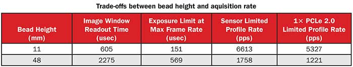
In practice, two of these three constraints will limit the system profile sampling speed. If a certain application has a tall bead, then a larger imager window that reduces pps must be used. The larger window increases both the readout time from the imager and the required PCIe bandwidth to transfer the images.
Finally, the application engine must be capable of accessing and processing bead profile shapes at high rates and, on average, not fall behind the vision engine acquisition rate. The circular image buffer in CPU memory provides some elasticity but, ultimately, the acquisition speed may be limited by the processing speed. The highest speeds are achieved with a combination of a SoM with the latest multicore processor, intelligent memory management and highly optimized algorithms.
High-speed and high-fidelity 3D inspection of adhesive beads can be achieved in a compact, robust, flexible, embedded vision design. Higher bandwidth and low cost goals can be met on an individual application basis by using more sophisticated (or economical)
SoMs and FPGAs that support faster (or slower) DMA interfaces. This results in highly tailored solutions that are scalable and low cost.
Meet the authors
Dave Kelly is vice president of research and development at Coherix Inc., with more than 25 years’ experience developing embedded vision systems for industrial and military applications; email: [email protected].
Andres Tamez is an embedded specialist and electronics manager at Coherix Inc.; email: [email protected].