As single-wavelength data rates are anticipated to approach 1 Tb/s, silicon photonics will enable the tightly coupled optics and electronics necessary for success.
CHRISTOPHER DOERR, ACACIA COMMUNICATIONS INC.
The simplest form of fiber optic
communication is coupling a laser to one end of a fiber, turning the laser on and
off to transmit ones and zeros, and connecting a photodetector to the other end to record the photocurrent. This simple modulation format is called on-off keying (OOK), and the reception is called direct detection.
Coherent communication
Besides optical power in single-mode optical fiber, phase and polarization are two additional orthogonal dimensions that
can be used to transmit information. Coherent communication uses these three dimensions, increasing the fiber’s data-carrying capacity by at least a factor of four in gigabits per second (Gb/s). Today, a capacity increase of a factor of 12 is deployed, which is achieved as a result of the receiver’s ability to read the amplitude and phase of the signal. Equalization permits practical complex multilevel modulation, such as 16-QAM (quadrature amplitude modulation) (Figure 1).
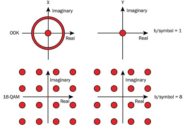
Figure 1. Data constellations showing the signal locations in the complex plane (real and imaginary axes). Single-polarization on-off keying (OOK) and dual-polarization 16-QAM (quadrature amplitude modulation). Courtesy of Acacia Communications Inc.
Coherent communication mixes the
received signal with a reference laser, called the local oscillator, in high-speed photodetectors. While optical coherent communication is a relatively old concept (dating from the 1980s), it only became widespread when advancements in CMOS processing reduced the digital signal processing (DSP) power sufficiently to process 100-Gb/s signals, circa 2010. Since then, the progress has been remarkable, with coherent solutions experiencing an exponential decrease in power consumption, size, and cost of ~40 percent per year (Figure 2).
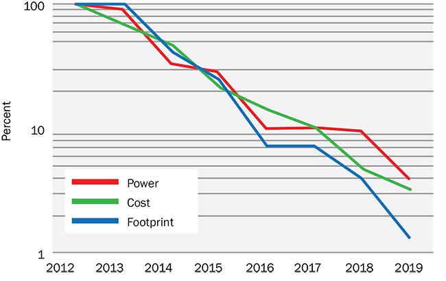
Figure 2. Power, cost, and footprint reduction in coherent communications per data transmission rate. Courtesy of Acacia Communications Inc.
Silicon photonics
Silicon (Si) is predominant in electronics because it is the most abundant material in the Earth’s crust. It is strong, easy to grow into large and low-defect crystals, has an excellent oxide, and has relatively high electron and hole mobilities. Its oxide, SiO2, has such desirable properties that it has led to silicon-on-insulator (SOI) wafers. An SOI wafer is made by bonding two oxidized silicon wafers together and removing most of one of the wafers. This results in a thin, perfect crystalline silicon layer on top of a near-perfect insulator, all on a large (typically 12-in.-diameter) silicon wafer. SOI wafers are used in electronics to make transistor circuits with extremely low leakage for low-power electronic applications.
Fortunately, silicon is optically transparent in the O- and C-bands (1230 to 1360 nm and 1530 to 1565 nm, respectively) — the primary wavelength regions used in fiber optic communications1. Optical waveguide losses in silicon can be as low as 0.2 dB/cm, making total propagation losses <1 dB for most practical
silicon photonic devices. The high refractive index contrast between silicon (3.48) and silicon dioxide (1.45) allows for very tight optical confinement and thus very compact devices, such as optical transceivers, with the opportunity for strong gratings, polarization splitters, and rotators. A cross section of a typical silicon waveguide is shown in Figure 3a. Modulators can be made by doping the silicon to make p-n junctions in the waveguide and changing the depletion width via an applied voltage (Figure 3b)2. Photodetectors can be made by growing germanium (Ge) on top of the silicon (Figure 3c)3. Ge is suited for photodetectors because it is nearly lattice-matched to Si (4 percent mismatch), and it has a narrower bandgap than Si, allowing it to absorb light in the O- and C-bands.
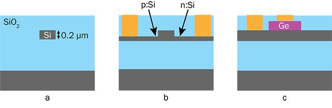
Figure 3. Silicon waveguide structures: passive waveguide (a); modulator illustrating junction between p-doped semiconductor and n-doped semiconductor, which acts as a diode (b); and photodetector (c). SiO2: silicon dioxide; Ge: germanium. Courtesy of Acacia Communications Inc.
The silicon photonic platform can be made with extremely high yield because of the near-ideal starting wafers and the maturity of silicon processes developed for electronics. These desirable features have led to the success of silicon photonics.
Silicon photonics, for all its benefits with functionality and yield, still lacks a monolithically integrated light source. Silicon and related group IV materials, such as Ge, are indirect bandgap semiconductors, and thus it is very difficult to create an efficient light source on silicon. Work-arounds have involved attaching III-V semiconductor lasers to the silicon, ranging from small subassemblies to oxide-to-oxide bonding chiplets at the wafer level.
As bit rates increase and the amount of electronic and photonic copackaging increases, integrating the laser into the silicon becomes less desirable. This is because the electronics dissipate considerable heat at high bit rates, and high temperatures significantly reduce the laser efficiency. Keeping the laser separate as an “optical power supply” thus provides an advantage. This approach can be especially beneficial for coherent transceivers, where DSP power dissipation can be high.
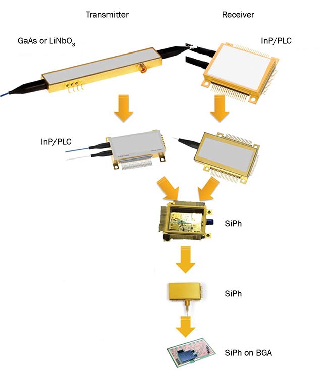
Figure 4. Coherent transceiver evolution. GaAs: gallium arsenide; LiNbO3: lithium niobate; InP: indium phosphide; PLC: planar lightwave circuit; SiPh: silicon photonics; BGA: ball grid array. Courtesy of Acacia Communications Inc.
Coherent transceivers have evolved, from LiNbO3 (lithium niobate) and GaAs (gallium arsenide) modulators with InP (indium phosphide) and silica PLC (planar lightwave circuit) receivers to single-chip silicon photonic transceivers (Figure 4)4. This single-chip transceiver contains all the optical elements of a coherent transceiver except the laser, and includes polarization splitters and rotators, high-speed modulators, high-speed photodetectors, monitor photodetectors, and variable optical attenuators.
Silicon photonics has many benefits in high-volume applications because it can leverage fab resources shared with the electronics industry.
As recently as 2012, silicon photonic coherent transceivers were packaged inside hermetically sealed gold-plated boxes. Manufacturers are now transitioning to chip-on-board packaging, which follows the trend of electronic circuit packaging and offers tremendous cost reduction. A silicon photonic coherent transceiver on a BGA (ball grid array) substrate can now survive both solder reflow and a nonhermetic environment (Figure 5)5.
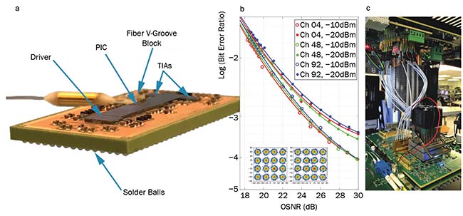
Figure 5. Silicon photonic coherent transceiver in a ball grid array (BGA) package and corresponding results. Photograph of the optoelectronic BGA device (a); measured performance of 200-Gb/s 16-QAM transmitted and then received by the device; specifically bit error ratio versus optical signal-to-noise ratio (OSNR) and the constellations (b); test platform of the device. The device is in the BGA socket (c). PIC: photonic integrated circuit; TIAs: transimpedance amplifiers. Courtesy of Acacia Communications Inc.
Since the late 1980s, silicon photonics companies have been making optical transceivers (Figure 6). Commercialization started with Oclaro Inc. in 1988 (then known as Bookham Technology). By the early 2000s, multiple companies, including Luxtera Inc., Lightwire Ltd., and Mellanox Technologies, had begun making short-reach (<2 km) direct-detection transceivers. Acacia Communications Inc. introduced commercial coherent transceivers in 2012, beginning with long-haul (>100 km) and moving progressively toward shorter and shorter reaches.
Future directions
For all its benefits with functionality and yield, silicon photonics still lacks a monolithically integrated light source.
As of 2018, coherent solutions supporting up to 600 Gb/s per wavelength are being deployed using the latest in DSP and optical technologies. Within three to five years, single-wavelength data rates will likely exceed 1 Tb/s, which will further reduce the cost per bit of transport. These higher data rates will require closely coupled optics and electronics that leverage the benefits of silicon photonics.
Short-reach links (<2 km) of 400 Gb/s per transceiver (100 Gb/s per wavelength) are just being introduced. The next step may bring 800 Gb/s per transceiver using eight lanes of PAM4 (4-level pulse amplitude modulation). Achieving more than 100 Gb/s per wavelength with direct detection will be difficult, however, so coherent solutions may make their way into the data center for rates above 800 Gb/s. Supporting this trend will require low-cost, coherent-grade lasers. Silicon photonics offers many benefits in these high-volume applications because it can leverage fab
resources that are shared with the electronics industry, ramp up quickly, and achieve high yields.
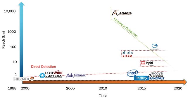
Figure 6. History of silicon photonic transceiver companies. All trademarks, service marks, logos, company names, and product names are the property of their respective owners and are used for identification purposes only. Use of these names, logos, and brands does not imply endorsement. Courtesy of Acacia Communications Inc.
And as Ethernet switch capacities grow to 50 Tb/s, the communications industry is increasingly interested in copackaged optics. Silicon photonic interconnects could be directly connected to switches through XSR (extremely short-reach) links, which are defined as 5 cm by IEEE. Lasers may be located separately, acting like optical power supplies for the transceivers. This approach would significantly leverage the benefits of silicon photonic technology.
Meet the author
Christopher Doerr, Ph.D., is associate vice president of advanced development at Acacia Communications Inc. He has more than 20 years of experience in optical communications. A fellow of IEEE, OSA, and Bell Labs, he has received multiple awards, including the IEEE William Streifer Scientific Achievement Award; email: [email protected].
References
1. R. Soref and B. Bennett (1987). Electrooptical effects in silicon. IEEE J Quantum Electron, Vol. 23, Issue 1, pp. 123-129.
2. A. Liu et al. (2007). High-speed optical modulation based on carrier depletion in a silicon waveguide. Opt Express, Vol. 15, Issue 2, pp. 660-668.
3. D. Ahn et al. (2007). High performance, waveguide integrated Ge photodetectors. Opt Express, Vol. 15, Issue 7, pp. 3916-3921.
4. C.R. Doerr et al. (2014). Single-chip silicon photonics 100-Gb/s coherent transceiver. Opt Fiber Commun Conf Postdeadline Pap, paper Th5C.1.
5. C. Doerr et al. (2017). Silicon photonics coherent transceiver in a ball-grid array package. Opt Fiber Commun Conf Postdeadline Pap, paper Th5D.5.