Dr. Reinhard Voelkel, Suss MicroOptics SA
Early inventions in the field of planar diffractive and refractive micro-optics date back more than a century. In 1891, Gabriel Lippmann invented “interference color photography,” later called Lippmann holograms. This invention was made without lasers and long before Dennis Gabor invented holography in 1948. Lippmann also invented “integral photography,” an autostereoscopic method to display 3-D images for observation with the naked eye.
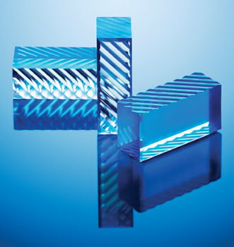
Double-sided microlens arrays manufactured by resist melting and reactive ion etching on 8-in. fused silica wafer. Courtesy of Suss MicroOptics.
Integral photography is based on a microlens array, in which each microlens acts like a miniaturized camera recording an individual subimage. Observing the developed photographic plate through a similar lens array, the superimposed subimages form an autostereoscopic integral image, or a 3-D image. Today’s most sophisticated 3-D television screens are based on this principle. TV screens of up to 60 in. diagonal, equipped with a huge microlens array perfectly matched to the LCD pixels, provide extraordinary 3-D television.
Another mature application is the fly’s-eye condenser, also referred to as the Köhler integrator, developed in the early 1940s to further improve the light uniformity of cinema film projectors. Similar microlens-based Köhler integrators are widely used in all kinds of illumination systems today. From lightweight microbeamers for smartphones to heavy laser machining systems for steel cutting, micro-optical components are used to precisely shape the light without loss.
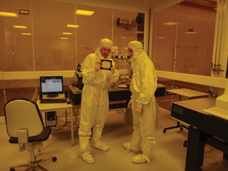
Reinhard Voelkel, CEO of Suss MicroOptics, explains the micro-optical light homogenizer in the MO Exposure Optics illumination system for an MA300 mask aligner to Carlos Lee, general director of EPIC. Courtesy of Carlos Lee.
Over the past hundred years, many researchers published and patented inventions where micro-optics were a decisive key element. These often were brilliant ideas, but few could be realized, and even fewer saw commercial success. For early micro-optics applications, the insurmountable entrance barrier was the availability of suitable micro-optical elements for reasonable costs. Piece-by-piece fabrication by engraving or polishing was very time-consuming and expensive, and the arrays had to be uniform.
Later, glass molding, casting and pressing were used. Often, the quality of these microlens arrays remained poor. Surface roughness, defects, lens profile accuracy and nonuniformities in the array constrained their field of applications to illumination tasks.
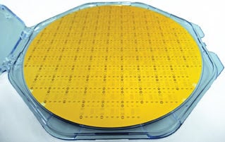
Wafer (8 in.) with VGA lenses on blue tape after dicing. The wafer-level cameras consist of two wafers with micro-optics (double sided) manufactured by wafer-scale imprint technology and wafer-level packaging. Courtesy of Heptagon.
Micro-optics was considered a very promising future technology, but difficult to manufacture. This situation changed with the rapid progress of microstructuring technology in the second part of the last century, strongly influenced by the semiconductor industry and the upcoming wafer-based “planar” manufacturing technology.
Semiconductor industry
In the semiconductor industry, the term “wafer” appeared in the 1950s to describe a thin, round slice of semiconductor material, typically germanium or silicon. The breakthrough for planar wafer manufacturing in the semiconductor industry came with the invention of the “planar process” by Jean Hoerni, a founder of Fairchild Semiconductor in 1957.1
The next decisive invention was to connect these transistors and form integrated circuits or microchips. Robert Noyce, also a founder of Fairchild and, later, Intel, patented his planar integrated circuit (IC) in 1959, and Fairchild started IC manufacturing in 1960.2 Hundreds, thousands and later millions of electronic components could be manufactured in parallel. Replacing discrete piece-by-piece electronic fabrications by Fairchild’s planar process revolutionized the semiconductor industry.
This was the start of the integrated circuit explosion in what is now called Silicon Valley, which created more than 30,000 new workplaces within only a few years. Soon, the rapidly growing semiconductor industry triggered a large request for manufacturing and testing equipment; the semiconductor equipment industry started around the semiconductor fabs. The industry has moved from 1-in. wafer size to 300 mm within the past 50 years. Wafer-based manufacturing technology made incredible progress from 20-µm resolution in the early 1960s to <22 nm today.
Planar micro-optics
Planar manufacturing technology from the semiconductor industry also had a considerable impact on micro-optics manufacturing. Gabor’s invention of holography enabled the recording of gratings in a planar photographic plate.
In the mid-1960s, Adolf W. Lohmann made the next step by combining computers, plotters and photography to manufacture more complex optical functions in what he called a computer-generated hologram. Dry plasma etching technology to transfer micro-optical structures from photoresist into glass wafers was invented in the 1970s.
In the mid-1980s, Zoran Popovic proposed a microlens fabrication technology based on microstructuring of the photoresist by photolithography and a subsequent resist melting process. Reactive ion etching was now available to transfer the micro-optics from photoresist into wafer bulk material such as fused silica, silicon or borofloat glass.
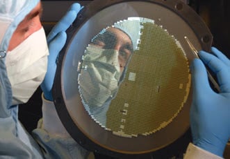
(Above) Photograph of 8-in. wafer (fused silica) populated with different diffractive and refractive micro-optical elements for focusing and beamsplitting. The wafer is coated with a gold mirror layer. Courtesy of Suss MicroOptics.
Planar optics was one of the most promising future technologies in the 1980s. Well-funded government programs triggered a micro-optics hype in all industrial countries. The opportunities included not only optical computing, but also many other applications for planar micro-optics in medicine, biology, optical communication networks and more. The optics community hoped to repeat the semiconductor hype in generating infinite growth and wealth of a planar optics industry similar to the integrated circuit explosion in Silicon Valley.
The first companies for micro-optics manufacturing on the wafer scale appeared in the 1990s. However, neither the optical computer nor the later “photonics hype” really took off. Micro-optics could not redo what the semiconductor industry had done. The fundamental difference is that electronics allows complete devices to be built – including the input sensor, CPU (central processing unit), memory and output, a display, sound or movement. Optics and micro-optical elements are typically only parts of a larger mechanical or electronic device used to redirect, shape or switch the light.
Fortunately, they often are key enabling components that significantly improve the performance of the complete device. Micro-optics is an established mature product, but it remains a niche, without big growth and big business. Even today, the supplier base for micro-optics is relatively small. Even large multibillion-dollar companies purchase their micro-optics from small and medium-sized suppliers.
Micro-optics allows illumination light to be precisely shaped for imaging and projection systems. Micro-optical fiber couplers, gratings for wavelength multiplexing and switches are essential components for high-speed communications systems. Micro-optics allows mass production of high-quality miniaturized optical systems at very attractive costs, and the list of innovations using micro-optics is long. It’s not such a new phenomenon. A hundred years ago, researchers invented devices and systems based on micro-optics, but most of these inventions failed because no suitable fabrication technology for the micro-optics was available.
Wafer-level manufacturing
Today, wafer-level manufacturing of micro-optics is typically in 6-in. or 8-in. (200 mm) wafer technology. Whereas 6 in. and 8 in. are old-fashioned technology for semiconductor manufacturing, they are perfectly suited for micro-optics. Compared with semiconductors, the lithography requirements for micro-optics are much more relaxed. Typically, a minimum feature size of 0.5 to 0.8 µm is sufficient for diffractive optical elements (DOEs). Thus, older and much less expensive i-line steppers from the 1990s are well suited for this task. Novel technology trends, such as wafer-level packaging (WLP), thin-wafer handling, 3-D chip
integration (3D-IC) and through-silicon via (TSV), are also available for 8-in. wafer manufacturing equipment.
Although manufactured with “antiqued” lithography steppers, DOEs play a very decisive role in the illumination systems of most sophisticated high-end DUV lithography steppers. Typically, a lithography stepper comprises four to six micro-optical components for precise laser beam and pupil shaping. Lithography enhancement techniques such as customized illumination and source-mask optimization are based on micro-optical components. Micro-optics elements had a major impact on the reduction of aberrations and diffraction effects in projection lithography, enabling a resolution enhancement from 250 nm to <40 nm within the past decade.
Microlens Köhler integrator for mask aligner illumination systems. Courtesy of MO
Exposure Optics.
Wafer-level stacking
Kenichi Iga and his colleagues attracted attention in the early 1980s with their idea of “stacked planar optics.”3 In the early 1990s, the first systems requiring a stack of microlens wafers were built; e.g., a 1:1 microlens projection lithography system for mask aligners imaging a photomask to a wafer located at a large distance.4
The most critical step for such early wafer-level projection systems was the proper alignment of multiple wafers. Wafer-level cameras combining 6-in. micro-optics and thinned CMOS imagers (back-side illumination) were developed in 2002.5 Wafer-level cameras for low-cost applications such as mobile phone cameras and disposable endoscopes have gained much in popularity recently. For low-cost systems, the micro-optical components are usually fabricated by microlens imprint lithography,6 which uses soft or hard stamps to imprint microlens arrays in polymer or Ormocer on a full-wafer level. The microlens wafers are then mounted by WLP to wafer-level optics modules.7
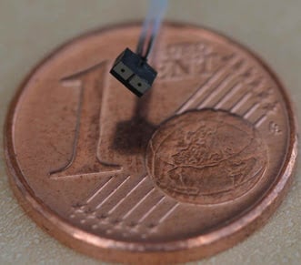
Stereo-wafer-level camera serving for disposable endoscopes. Courtesy of NanEye Stereo Module, www.awaiba.com.
The next step is wafer-level integration (WLI), combining wafer-level micro-optics with optoelectronic components such as photodiodes, LEDs or lasers arranged and mounted on wafer level. The WLI approach gained much success recently for manufacturing high-volume components integrated in the latest generations of smartphones.
On one 8-in. wafer, up to 5000 lenses can be fabricated simultaneously. The process chain includes lithography for apertures, double-sided and aligned replication of lenses, stacking of wafers, automated optical testing and wafer dicing. Providing miniaturized optoelectronic modules for smartphones allowed the current industry leader, Heptagon, to double its workforce within one year to almost 1000 employees.
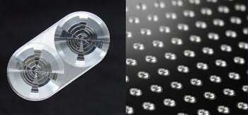
LED flash lenses for mobile phones, fabricated by wafer-level UV replication on wafer level. Courtesy of Heptagon.
Outlook
Wafer-level fabrication of micro-optics is already a mature technology. Equipment, processes and standards from the semiconductor industry have been used to establish reliable and repeatable fabrication processes to provide high-quality micro-optical components for many applications.
The important role of wafer-level micro-optics is based on various motivations: miniaturization, high functionality, packaging and integration aspects. Recent trends in the semiconductor industry – thin-wafer handling, 3D-IC/TSV, subwavelength metal gratings for color filtering in CMOS technology, etc. – will have a significant impact on the prospering micro-optics industry in the near future. Making microchips smaller and the Internet faster; increasing smartphone battery life, night vision and thermal vision for cars; and improving surgery and medical diagnostics, car manufacturing, consumer goods, clean technology and health care – micro-optics is a key enabling component. Typically, micro-optics is not seen – but we are ubiquitous.
Meet the author
Dr. Reinhard Voelkel is the CEO of Suss MicroOptics SA in Hauterive, Switzerland; email: [email protected].
References
1. Jean A. Hoerni (1959). Method of manufacturing semiconductor devices, US Patent 3,025,589, filed May 1, 1959.
2. Robert Noyce (1959). Semiconductor device-and-lead structure, US Patent 2,981,877, ?led July 30, 1959.
3. Kenichi Iga et al (1982). Stacked planar optics: An application of the planar microlens. Appl Opt, Vol. 21, No. 19.
4. R. Voelkel et al (1995). Microlens lithography: A new fabrication method for very large displays. Asia Display’95, pp. 713-716.
5. EU-IST-2001-35366, Project WALORI, WAfer Level Optic solution foR compact CMOS Imager (2002-2005).
6. R. Voelkel et al (2008). Technology trends of microlens imprint lithography and wafer level cameras (WLC), 14th Micro-Optics Conference (MOC ’08, Brussels). Belgium Tech Dig, pp. 312-315.
7. M. Rossi et al (2003). Wafer scale micro-optics replication technology. Proc SPIE, Vol. 5183, 1-2.