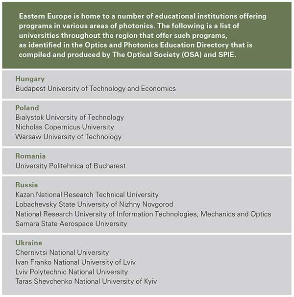
Universities and research institutions throughout Eastern Europe are stepping up to educate and produce future photonics leaders. Schools like the Warsaw University of Technology in Poland and Kazan National Research Technical University in Russia play a key role, as do research and support programs, such as the Romanian Institute of Science and Technology, which are emerging regionwide.
Eastern Europe, like many other regions, is putting great thought and effort into producing the next generation of photonics and optics researchers and engineers. Countries including Romania are working hard to keep up with the growing demand for experienced workers, not only in research, but also in technology transfer and applications.
“There is a lack of experienced technology transfer professionals,” said Alexandru Cabuz, project leader for Research for Industry, a Romania-based program offering technology transfer training for research institutions. The program is drawing on the expertise and support of platforms already established, including within institutions in Switzerland, in order to further develop Romania’s research and technology ecosystem. A number of other programs are working to serve the same purpose.
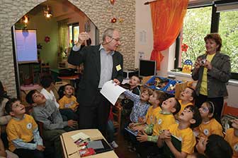
Demonstration of the difference between a torch and a laser, using the OSA Optics Suitcase, at the Happy Kids kindergarten in Râmnicu-Vâlcea, Romania. Courtesy of Dan Sporea.
But long before new technology is ready to incorporate into commercial development, more work is needed to move the region to the front of the industry pack. And it begins with education.
Education programs
Many universities and other education institutions are establishing programs and areas of study in photonics and optics; some are extensions of existing science-related study, while others are more recently established.
Some of the largest programs in the region are at the National Research University of Information Technologies, Mechanics and Optics (ITMO) in St. Petersburg, Russia. There are 300 optics and photonics students currently enrolled there, and about 3,000 studying optics-related fields. The school features six research centers — Intelligent Systems for Data Management and Processing, Technologies of Programming and Artificial Intelligence, Technologies of Highly Efficient Computing and Systems, Photonics and Optical Information, Optical Nanotechnologies, and Materials Optical and Laser Systems. In addition to core optics and photonics, students (undergraduate to doctoral) can focus on optical engineering, biomedical optics, fiber optic communications and optical electronic devices.
ITMO also has a very active Student Optics Chapter, which received the OSA Student Chapter Excellence Prize at the international OSA Student Leadership Conference in October.
Also in Russia is the Kazan National Research Technical University. Located in Tatarstan, there are more than 100 core optics and photonics students enrolled, in addition to nearly 200 students studying optics-related courses, according to the international Optics and Photonics Education Directory, compiled and produced by OSA and SPIE. Disciplines such as optical engineering, photonics, biomedical optics, and fiber optic communications (among others) are offered, with focuses in optical system design, optical systems for lasers, and laser and fiber spectrometers. This school has produced more than 80,000 graduates since its establishment in 1932, and provides a multilevel continuous training system for professional development beyond classroom walls.
Similar academic programs are available to the west of Tatarstan, at the Budapest University of Technology and Economics in Hungary. Its Faculty of Natural Sciences (established in 1998) has emerged as a strong program in recent years, with 65 Ph.D. students currently studying photonics, optics, optical engineering and physics. Students can also study fiber optic systems, time-resolved fluorescence spectroscopy of biological materials, optical measurement, laser materials processing, IR differential absorption lidar, displays and photovoltaics in the program. And the school is growing, too, with nearly 40 undergraduate students immersed in optics-related coursework; more than 20 are core optics and photonics students.
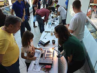
A young visitor at the Center for Science Education and Training (CSET) at the National Institute for Laser, Plasma and Radiation Physics, examines a newly introduced teaching kit about photovoltaic energy at the Researchers’ Night 2015 in Bucharest, Romania. Courtesy of Andrei Stancalie.
Romania’s University Politehnica of Bucharest is another robust institute offering a number of programs for optics and photonics students; there are currently more than 100 students exploring some type of optics- and/or photonics-related study. Specific disciplines include optical engineering, optical information processing, geometrical optics, photonics technologies and power sources, and fiber optics.
Travel 1,700 km (about 1,000 miles) north of Bucharest to find Warsaw University of Technology in Poland. The school’s Institute of Microelectronics and Optoelectronics (IMiO) offers studies in microwave and image photonics, optoelectronics, microelectronics, and nanoelectronics, among others. And its newer program, Faculty of Physics (established in 1999), offers more focused study in areas such as optics, photonics, semiconductors, structural research and solid-state ionics.
IMiO is involved in educational training events, as well, hosting a workshop in May for companies, universities and research institutes, led by Photonic Advanced Research and Development for Integrated Generic Manufacturing (PARADIGM), a project funded by the Seventh Framework Programme of the European Commission (EU). The scope of the Eastern European Workshop on Generic Integration Technologies for Photonics encompassed all aspects of the generic approach to photonic integration, according to Ryszard Piramidowicz, deputy director of research at IMiO, including Application Specific for Photonic Integrated Circuits (ASPICs) and indium phosphide-based integrated photonics.
The general concept and all consecutive stages of the generic manufacturing chain were presented and discussed in detail by top-level experts in the field, he said, which were “complemented by a tutorial on designing photonic integrated circuits with dedicated CAD software.” Also presented were capabilities of different technological platforms, and financial mechanisms enabling and supporting further development of integrated photonics were also discussed.
ASPIC users presented “their own experience in exploitation of the generic foundry platform and cooperation with the PARADIGM consortium and the Eastern Europe Design Hub in particular,” Piramidowicz said.
PARADIGM is an educational resource for photonics students, aiming to create “generic integrated technology for the research, development and manufacturing of [ASPICs].” According to the PARADIGM website, this cost-effective, versatile platform technology will be “adapted to the capabilities of available, mature, high-performance fabrication processes,” rather than adjusting it for individual, specific applications.
The new platform is expected to “significantly reduce the fabrication cost of photonic chips, as well as provide compact and energy-efficient devices.” It also could assist smaller companies by providing affordable access to cutting-edge technology, in turn allowing such companies to create ASPICs for sensors, metrology, data communications and others.
Yet another educational resource is the Center for Science Education and Training (CSET) at the National Institute for Laser, Plasma and Radiation Physics (INFLPR) in Romania. Established more than 10 years ago, according to Dan Sporea, of INFLPR, and a coordinator at the center, CSET supports science education at the pre-university level (from kindergarten to high school). A 2007 case study that Sporea co-authored, International Photonics Training, cited the establishment of an international collaboration with the New England Board of Higher Education, based in Boston. CSET coordinated with a Romanian high-school science teacher to participate in a 12-week Introduction to Photonics lab-based professional development program, funded by an Advanced Technological Education (ATE) grant from the (U.S.) National Science Foundation; this teacher later shared what she learned with fellow high-school-level and community-college educators, with the intent of helping them carry on the lessons and information to their students.
“Along the years we delivered courses for teachers … and organized science fairs, contests for school students, [and] workshops,” Sporea said. “We [also] distributed to schools the Galileoscope Kit, several types of data loggers, mini instruments for light pollution monitoring [and] UV data loggers, and now they are running their own investigations.”
He added that CSET has also offered a virtual project and contest for schoolchildren, in collaboration with Judith Donnelly, formerly of Three Rivers Community College in Connecticut, in which they were tasked with illustrating (via drawings and/or photos) the vital importance of the sun.
The i-BEST (Inquiry-Based Education in Science and Technology) project ties into CSET and other such initiatives, Sporea said. I-BEST “addresses different aspects of teaching sciences in order to have a long-term impact.” It is a training tool for educators and students, sharing with them the processes needed to develop their own research projects related to monitoring weather, environmental changes, noise, water quality and risk caused by UV radiation. This collaborative platform helps pre-college students share results of various science projects, Sporea said. And it provides translations of modules from the American project Hands-on Optics, with distribution of optics kits that include simple spectrometers and digital microscopes. Teaching aids on areas such as photovoltaics are offered for “inquiry-type activities,” and students can also participate in the annual Science Education in School international conference.
Research support
Photonics education extends beyond university walls. Out-of-classroom settings (labs, research institutes, photonics and optics companies, etc.) and industry organizations are important, too, providing support for students and researchers.
The Romanian Institute of Science and Technology (RIST) is a nonprofit independent research organization established in 2009 to provide “appropriate institutional and administrative support for world-class scientists that would like to work in Romania and are not satisfied by the conditions offered by existing Romanian research institutions.”
RIST helps to promote optics and other photonics-related work in Romania, bridging the gap between research and industry through various programs that support technology transfer and entrepreneurship within the country’s advanced research institutions. Initiatives are in place, such as at the University Center for Optics and Photonics Engineering, led by the University Politehnica of Bucharest, with a focus on engineering optics and photonics; optoelectronics (theoretical and experimental); lasers and applications in engineering optics (atomic and nuclear); and photonic devices and systems. RIST helps coordinate support for research projects in these and other sciences by way of European structural funds awarded by the Romanian National Authority for Research and Innovation.
Romanian-based Research for Industry is another support mechanism for researchers and students. Research for Industry, a RIST program developed in conjunction with the Technology Transfer Office (TTO) of the Swiss Federal Institute of Technology (EPFL) in Lausanne, Switzerland, is the only professional resource for technology transfer training and consulting for Romanian research institutions, said program director Alexandru Cabuz.
“Our partnership with the Tech Transfer Office of [EPFL] ensures that we implement the best practices, tried and tested in one of the most highly performing technology institutions in the world,” he said. “There is a lack of experienced technology transfer professionals in Romania, and we are bringing the experience accumulated in the Swiss ecosystem to bear for supporting the development of the Romanian ecosystem.”
Romanian research institutions benefit from the “know-how and good practices” reaped from the EPFL-TTO, particularly the drafting and negotiation of industrial contracts, including consortium agreements for Romanian or European funds. Research for Industry also offers Romanian institutions support for managing intellectual property in international markets. Training for tech transfer managers in Romanian institutions is available, as well, in addition to support for students and scientists interested in founding startups, through connections with entrepreneurial ecosystems in Switzerland, U.K. and Germany.
“Industry can use our deep knowledge of the Romanian research system and our extensive database of research labs to identify and initiate contact with research labs active in the areas of interest to them,” Cabuz said, adding that the organization assists with intermediate negotiations, “which has significant value since the expectations of most Romanian scientists are disconnected from the realities of the European and international markets, and from good practices in intellectual property.”
Continuing education through research
The EU several years ago endowed nearly €180 million (about $193 million) for construction of a new laboratory in Romania for study of laser-based nuclear physics. Called Extreme Light Infrastructure-Nuclear Physics (ELI-NP), the project began as part of a broader initiative with the Czech Republic and Hungary to form a pioneering European research consortium. Implementation of the ELI-NP program began in 2013, and will conclude at the end of 2018. The initiative involves research and academic institutions from member states and others from the business sector, and will be part of the first pan-European multidisciplinary network to host the most intense lasers available.
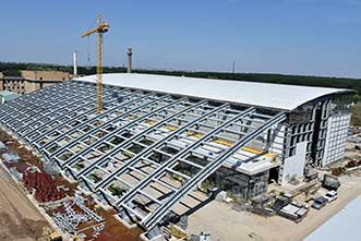
The Extreme Light Infrastructure-Nuclear Physics (ELI-NP) facility, currently under construction in Magurele, Romania. Courtesy of ELI-NP.
The ELI-NP consists of two major components:
• A very high intensity laser constructed by combining the beams of two 10-petawatt Apollon-type lasers, “to get intensities of the order of 1023 to 1024 W/cm2 and electrical fields of 1015 V/m.
• A very intense (1013 γ/s), brilliant γ beam, 0.1 percent bandwidth, with Ev > 19 MeV, which is obtained by incoherent Compton back scattering of a laser light off a very brilliant, intense, classical electron beam (Ee > 700 MeV) produced by a warm linac.
This infrastructure will create a new European laboratory and platform allowing focus in a broad range of sciences.
It will all be housed in a facility in Magurele, Romania, which is currently under construction.
“The building construction will be finished in the beginning of next year [2016],” said ELI-NP project director Dr. Nicolae-Victor Zamfir, who is also director general of Horia Hulubei National Institute of Physics and Nuclear Engineering (IFIN-HH). “The components of the first 10-PW laser are delivered, the first section of the gamma beam is ready, and we started to implement the Technical Design Reports of the experimental set-ups.”
The Center for Advanced Laser Technologies (CETAL), under the umbrella of the National Institute for Laser, Plasma and Radiation Physics (INFLPR) — an independent research institution established by the Romanian government — is a research infrastructure designed for researchers working with photonics technologies, said Sporea, deputy technical director of the project. It offers access to high-performance laser equipment for universities and other educational and research institutes.
CETAL comprises three labs:
• Laboratory of High-Field Laser Physics — features a PW-class laser.
• Laboratory of Laser Material Processing — features several laser materials processing units produced by Trumpf Inc.
• Photonic Investigations Laboratory — dedicated to optical spectroscopy, THz spectroscopy, LIBS-based investigations, Raman spectroscopy, mid-IR spectroscopy, shock and vibrations tests and measurements, and optical fiber sensing.
The CETAL infrastructure has been established on the Magurele platform.
CLARA (the EU Center of Excellence in Laser and Radiation Applications), developed jointly by INFLPR and the IFIN-HH, is a project that focuses on the development of research infrastructure, and is a Key Enabling Technology (KET) cluster. Described in a 2014 paper authored by Marius Eugen Opran, director of the Center for Technology Transfer and Innovation at INFLPR and promoter of the project (presented at the Reunion of the Assembly of General Directors of National R&D Institutes at Magurele-Bucharest), CLARA essentially governs ELI-NP and CETAL, supporting fundamental and applied research, innovation, applications and technology transfer, and ultimately product development. CLARA is structured in numerous components, from research to evaluation and testing; from R&D investments to education and training.
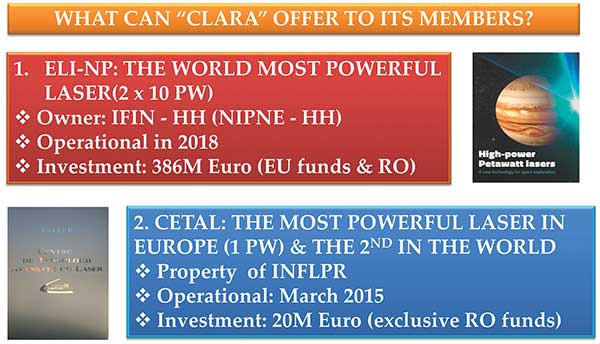
CLARA (the EU Center of Excellence in Laser and Radiation Applications), developed jointly by the National Institute for Laser, Plasma and Radiation Physics (INFLPR) and the Horia Hulubei National Institute of Physics and Nuclear Engineering (IFIN-HH), all in Romania, supports fundamental and applied research, innovation, applications and technology transfer, and ultimately product development. Courtesy of Marius Eugen Opran.
Conference learning
SPIE’s Photonics West is the largest international laser, photonics and biomedical optics conference, attracting many researchers and companies from Eastern Europe. Thousands of exhibitors from all areas of photonics offer new product information and demos, educational courses and sessions; talks by photonics industry experts are also held during the conference. The 2016 Photonics West will be held in San Francisco, Feb. 13-18.
There are other international events that offer the same benefits for the industry. Among them is SPIE Photonics Europe, set for April 4-7, 2015 in Brussels. This research and educational conference and technology exhibition showcases “the latest in photonics, optics, lasers, and micro/nanotechnologies,” according to SPIE, and now includes new subconferences on quantum optics, graphene and 2D materials.
PITTCON is another universally recognized event, to be held in Atlanta in March 2016, offering a hands-on look at innovative laboratory instrumentation, live product demos and educational sessions with technical experts. Just a couple of weeks later, from March 20-24, the Optical Fiber Communication Conference and Exhibition (OFC) is held in Anaheim, Calif. It annually brings together researchers, students, companies, government agencies and others to share “insights and inspiration on the major trends and technology advances affecting the industry.” Photonics: World of Lasers and Optics, held in Russia, touts more than 10,000 visitors annually. The event features hundreds of exhibitors, and offers a technological platform in which to learn about the latest trends in lasers and optoelectronics.
The Micro- to Nano-Photonics IV– ROMOPTO conference is an “international scientific event dedicated to optics and lasers,” according to OSA. This annual conference offers a forum in which experts working in optics and lasers can share their work and experiences, as well as interdisciplinary exchanges.
These and other such conferences are only a piece of the puzzle. To fill in the rest, continuing education via universities and research institutions across Eastern Europe, as well as programs such as ELI-NP, CLARA, CETAL, INFLPR and Research for Industry are crucial. The advancement of photonics in Eastern Europe, and around the world, begins with education and professional development.