Subwavelength channels enable efficient lightguiding, suggesting the feasibility of ultracompact plasmonic components and a new class of integrated optical circuits.
Dr. Sergey I. Bozhevolnyi, Aalborg Universitet
Modern communications systems must deal with huge amounts of data at ever-increasing speeds. In doing so, they try to use the best features of electronic and optical circuits. Electronic circuits are tiny, but their operation speed is limited. Optical circuits are much better at transmitting data at high speed, but their sizes are limited by diffraction — that is, propagating light cannot be squeezed in the lateral cross section below its wavelength in the medium.
Channel plasmons promise both the compactness of electronics and the speed of optics. Recent experiments have shown that channel plasmons propagate along the bottom of subwavelength grooves cut into a metal surface with strong confinement and low propagation loss, making them likely candidates for the realization of ultracompact photonic components.
Channel plasmons belong to the family of surface plasmons, which are electromagnetic excitations that are bound to and propagate along a metal/dielectric interface (Figure 1a). Surface plasmons feel the effects of both media and are characterized by the wavelength λsp, which is less than the wavelength in the dielectric.1
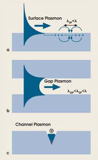
Figure 1. The schematic shows a surface plasmon field distribution, indicating the electric field directions and the surface plasmon wavelength, λsp; i.e., the spatial period of surface plasmon field oscillations (a). λ is the optical wavelength. Coupled surface plasmons create a gap plasmon with a shorter wavelength — λgp — than that of the surface plasmons (b). A groove cut in metal supports a channel plasmon that can be viewed as a gap plasmon confined laterally by varying the gap width (c).
The main issue in the context of the application of channel plasmons for optical interconnects involves the strong confinement of the surface plasmon field in the cross section perpendicular to the direction of surface plasmon propagation.
To better understand the concept of channel plasmons, let us first consider gap plasmons: surface plasmon modes guided between two closely spaced metal surfaces so that surface plasmons associated with the individual metal surfaces become coupled (Figure 1b). Gap plasmons can be easily squeezed to subwavelength dimensions. Smaller gaps result in shorter-wavelength gap plasmons, although at the expense of greater propagation losses.2 Because the mode field is nearly constant and close to its maximum for subwavelength gaps, however, the propagation loss determined by the portion of field penetrating the metal is as small as it can be for a given confinement.
Now let us consider a straight groove, cut into the metal with a V-shaped cross section.
Getting in the groove
Light tends to concentrate in regions where its wavelength is shortest (e.g., where the refractive index is largest), ensuring plasmon field confinement at the bottom of the groove (Figure 1c).
The question thus becomes whether and how such grooves can be used to manipulate the propagation of plasmons. The possibility of guiding electromagnetic waves using a channel cut into an otherwise planar surface of a metal or polar dielectric solid characterized by a negative dielectric function was first considered by Alexei A. Maradudin of the University of California, Irvine, and colleagues 15 years ago. The concept recently was refined, taking into account retardation and losses.3
Extensive numerical simulations predicted that channel plasmons can be employed for efficient transmission around sharp bends.4 Our preliminary experiments showed that they exist and that, at telecom wavelengths, they propagate over tens of microns along straight subwavelength grooves milled in gold.5
In our latest experiments, we have demonstrated that channel plasmon guides indeed can be used for efficient large-angle bending and splitting of radiation.6 This enables the realization of ultracompact plasmonic components and paves the way for a new class of integrated optical circuits.
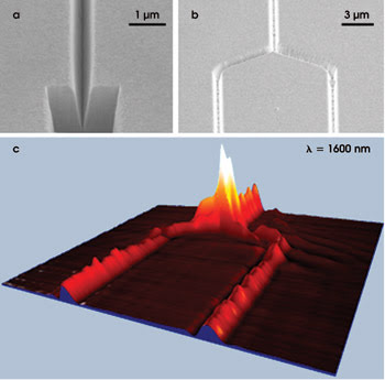
Figure 2. A scanning electron microscope images straight (a) and branched (b) 0.5-μm-wide, 1-μm-deep grooves supporting the propagation of a fundamental channel plasmon mode at telecom wavelengths. A near-field optical image shows the channel plasmon field intensity in the Y-splitter at the wavelength of 1.6 μm (c).
We fabricated various waveguide structures in a 1.8-μm-thick layer of gold deposited on a substrate of fused silica using high-resolution focused ion-beam milling. The structures consisted of V-grooves with angles of close to 25° and depths of 1.1 to 1.3 μm and included straight reference guides (Figure 2a), S-bends (i.e., curved bends connecting two parallel waveguides offset with respect to each other), Y-splitters composed of two mirrored S-bends (Figure 2b), Mach-Zehnder interferometers composed of two consecutive Y-splitters, and waveguide-ring resonators (Figure 3a). To characterize these plasmonic components, we used a scanning near-field optical microscope to map the field intensity of a channel plasmon as it propagated along the milled grooves, which were excited with end-fire coupling from a single-mode fiber.
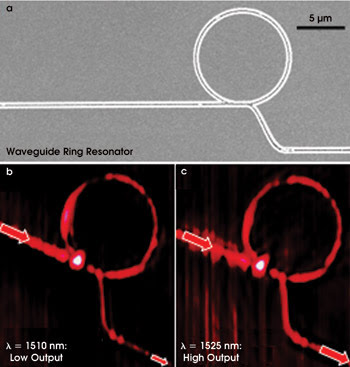
Figure 3. A scanning electron microscope images a waveguide-ring resonator with a radius of 5 μm (a). Near-field optical images of the channel plasmon field intensity in the waveguide-ring resonator at wavelengths of 1.51 μm (b) and 1.525 μm (c) demonstrate the wavelength filtering effect.
We found that the fabricated structures performed well from 1425 to 1620 nm, exhibiting single-mode and subwavelength guiding with overall losses of a few decibels and thus robustness to small variations in structural parameters. Moreover, waveguide-ring resonators with a footprint of only 200 μm2 exhibited wavelength-dependent transmission due to interference between a circling channel plasmon and an incoming one (Figures 3b and 3c), demonstrating that such components can be used for wavelength filtering with a bandwidth of ~40 nm.
It must be emphasized that there always will be a trade-off between the plasmon field confinement that is needed to decrease the bend losses and crosstalk and the propagation loss. The search for the best configuration, therefore, might never end. However, our latest findings help to narrow this search by providing a solution to the problem and elucidating the main features to be sought.
This solution already is suitable for practical applications, such as ultracompact optical interconnects — bearing in mind that channel plasmons are bound to and propagate along metal surfaces, enabling the natural integration of plasmonic structures with electrical circuits.
Meet the author
Sergey I. Bozhevolnyi is a professor in the department of physics and nanotechnology at Aalborg Universitet in Denmark; e-mail: [email protected].
References
1. S.I. Bozhevolnyi and V.M. Shalaev (January 2006). Nanophotonics with surface plasmons — Part I. PHOTONICS SPECTRA, pp. 58-66.
2. K. Tanaka and M. Tanaka (Feb. 24, 2003). Simulations of nanometric optical circuits based on surface plasmon polariton gap waveguide. APPL PHYS LETT, pp. 1158-1160.
3. I.V. Novikov and A.A. Maradudin (July 15, 2002). Channel polaritons. PHYS REV B, 035403.
4. D.F.P. Pile and D.K. Gramotnev (May 2005). Plasmonic subwavelength waveguides: next to zero losses at sharp bends. OPT LETT, pp. 1186-1188.
5. S.I. Bozhevolnyi et al (July 22, 2005). Channel plasmon-polariton guiding by subwavelength metal grooves. PHYS REV LETT, 046802.
6. S.I. Bozhevolnyi et al (March 23, 2006). Channel plasmon subwavelength waveguide components including interferometers and ring resonators. NATURE, pp. 508-511.