
2D Material’s High Tunability Could Augment Optoelectronics Applications
Research into a 2D material has revealed information about its tunability and band gap, that could help scientists to isolate, enhance and manipulate its most desirable qualities. Potential applications for atomically thin 2D materials range from microchip components to superthin, flexible solar panels and display screens.
Researchers at Lawrence Berkeley National Laboratory (Berkeley Lab) measured previously hidden properties of the 2D semiconducting material molybdenum disulfide (MoS2), providing a precise band gap measurement for this material, uncovering a powerful tuning mechanism, and revealing an interrelationship between MoS2’s optical and electronic properties.
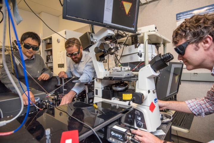
From left: Kaiyuan Yao, Nick Borys, and P. James Schuck, seen here at Berkeley Lab's Molecular Foundry, measured a property in a 2-D material that could help realize new applications. Courtesy of Marilyn Chung/Berkeley Lab.
The research team measured both the exciton and band gap signals, and then detangled these separate signals. Scientists observed how light was absorbed by electrons in the MoS2 sample when they adjusted the density of electrons in the sample by changing the electrical voltage on a layer of charged silicon that sat below the MoS2 monolayer.
Researchers noticed a slight “bump” in their measurements that they realized was a direct measurement of the band gap. Through additional experiments based on this discovery, they were able to demonstrate how the band gap was readily tunable by simply adjusting the density of electrons in the material.
Experiments showed the bandgap to be about 30 percent higher than researchers expected based on previous research. The team also quantified how the band gap changed with electron density, a phenomenon known as “band gap renormalization.”
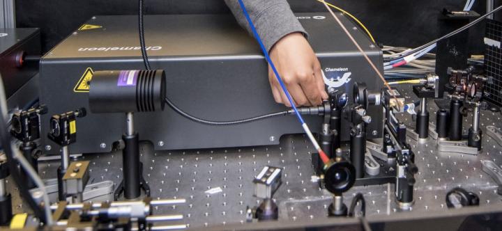
Kaiyuan Yao works with equipment at Berkeley Lab's Molecular Foundry that was used to help measure a property in a 2D material. Courtesy of Marilyn Chung/Berkeley Lab.
“The most critical significance of this work was in finding the band gap,” said researcher Kaiyuan Yao.
“That provides very important guidance to all of the optoelectronic device engineers. They need to know what the band gap is in order to properly connect the 2D material with other materials and components in a device.”
The researchers also resolved how to tune optical and electronic properties in the 2D material.
“The real power of our technique, and an important milestone for the physics community, is [how] to discern between these optical and electronic properties,” said researcher Nicholas Borys.
“The large degree of tunability really opens people’s eyes,” said P. James Schuck, who was director of the Imaging and Manipulation of Nanostructures facility at the Molecular Foundry during this study.
“And because we could see both the band gap’s edge and the excitons simultaneously, we could understand each independently and also understand the relationship between them,” said Schuck. “It turns out all of these properties are dependent on one another.”
MoS2, Schuck noted, is “extremely sensitive to its local environment,” which makes it a prime candidate for use in a range of sensors. Because it is highly sensitive to both optical and electronic effects, it could be used to translate incoming light into electronic signals and vice versa.
The technique that researchers adapted for use in their study of MoS2, known as photoluminescence excitation (PLE) spectroscopy, could lead to novel applications for this material, including ultrasensitive biosensors and tinier transistors. PLE spectroscopy also shows promise for pinpointing and manipulating properties in other 2D materials.
The team hopes to use a suite of tools and techniques at the Molecular Foundry to create other types of monolayer materials and samples of stacked 2D layers, and to obtain definitive band gap measurements for these materials.
“It turns out no one yet knows the band gaps for some of these other materials,” said Schuck.
The research was published in Physical Review Letters (doi. 10.1103/PhysRevLett.119.087401).
Published: September 2017