The ascent of stacked CMOS image sensors is permeating the imaging sector, giving rise to a host of applications previously unsupported by conventional and 2D sensor performance.
RAFAEL ROMAY-JUÁREZ, TELEDYNE IMAGING
CMOS manufacturing has undergone a significant transformation in the last 12 months. The manufacturing processes that even seasoned developers
regarded as fundamentally experimental
20, or even 10, years ago have come within reach of enabling an entirely new set of commercial applications. These breakthroughs are emerging in addition to the applications that industry innovators have already demonstrated owing to advancements in CMOS manufacturing processes.
Among the multitude of manufacturing processes currently under development, 3D stacking is prompting system developers, manufacturers, and end users to reconsider the possibilities of CMOS image sensor technology. A camera on a chip, an optical network on a chip, and even a neural network on a chip are now a part of a conversation that, finally, is inviting questions concerning when and not if such technology will enter into commercial markets.
A wave of differentiated applications necessitates improvements to individual features and overall system performance, especially for imagers. Such applications, spanning AI and industrial vision, are driving demand for 3D-stacked CMOS architectures. Courtesy of Teledyne Imaging.
With these possibilities on the near horizon, 3D-stacked CMOS, as an enabling technology, is imparting distinct advantages to systems. Often, systems powered by stacked CMOS can provide multiple advantages in combination. These include system miniaturization; higher responsivity and higher imaging speed with low power consumption; and more efficient high dynamic range (HDR) techniques and reduction of motion artifact. For AI applications and embedded systems
especially, the possibility to mix processes adds major value.
And, unlike many emerging technologies, 3D-stacked sensors will allow new solutions to be more cost-effective than the ones that they are poised to replace.
Industry markets are taking note of
this change in thinking. Yole Group predicted last summer that after a difficult 2023, the CMOS image sensor market will return to steady growth, reaching
$29 billion by 2028. The key driver for this growth will be more niche, differentiated applications, for which enhancements to individual features and overall performance will create competitive advantages and benefits.
The forecast also alludes to the vast number of industries that necessitate some degree of imaging technology. AI, 3D-gesture and face recognition, service drones and robots, and space navigation are among the sectors ripe with imaging needs. Advanced scientific applications, including those in spectroscopy, biomedical imaging, superresolution microscopy, near-IR tomography, ghost imaging, and quantum communications and cryptography are also well positioned for imaging-driven growth.
For the imaging sector, 3D-stacked CMOS technology is projected to help
define the future of product lines.
Already, almost every CMOS image
sensor in development at Teledyne Imaging is 3D stacked. In a short matter of time, it seems that this technology will start to function as a de facto standard in the sensor industry to help drive new levels of growth.
CMOS turned on its head
For many years, CMOS image sensors were front illuminated. The logic elements used to control the pixel array and its wiring surrounded the photosensitive area of the pixel, placing it at the bottom of a “metal tunnel” and reducing its field of view and sensitivity. Although this created an obvious performance disadvantage compared to legacy CCD sensors, CMOS simplified camera design for a
variety of other reasons, such as speed, cost, power, and the ability to add features onto the sensor chip. CMOS steadily replaced CCDs for many applications.
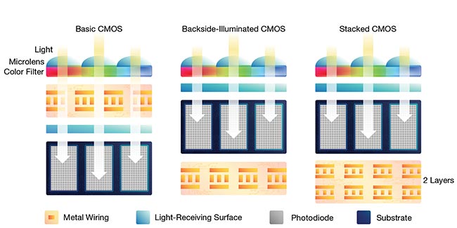
Back-side illuminated (BSI) sensor designs have bridged conventional or basic CMOS and initial iterations of stacked CMOS. The stacked designs offer added benefits for applications in industry, biomedical, and other sectors. Courtesy of Teledyne Imaging.
Though a relatively new advancement, the current stacked CMOS technology roadmap has its origins in the introduction of back-side illuminated (BSI) sensor designs. The development of BSI allowed designers to place the control and power lines of the pixel array directly behind the light-sensitive layer. This adjustment resulted in increased sensitivity automatically, thereby opening the door to 3D-stacked technology.
Beyond superior sensitivity, incorporating new functionalities underneath the sensing layer yielded a series of advantages. These include increased speed of control and readout, smaller footprint, and smaller power, as these functionalities were and continue to be manufactured via a more-advanced process than the pixel array.
The rise of BSI sensor designs also heightened the focus on additional aspects of CMOS sensor architectures. Designers placed a premium on overall shape as well as compact components. With conventional single-plane CMOS sensors, for example, there are some applications in which the pixel array is not the dominant piece of real estate, such as those that require capturing hundreds or more full-resolution frames per second, and/or those requiring substantial on-chip image post-processing. Its surrounding additional logic circuitry, and other pieces that assist the pixel array in meeting the demands of the application, can occupy as much area as the array itself. In these cases, with this circuitry moved below into the stack, the die size is normally defined by the pixel array.
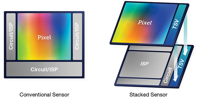
The inclusion of more circuitry, placed beneath the pixel layer, adds numerous ways to improve sensor performance for the end user (top). In this case, increasing the parallelism in the chip also becomes possible.
Added layers of circuitry under the pixel layer can be implemented in multiple (bottom). These nodes, such as for memory or logic, can also be smaller than in-pixel memory, enabling implementation of the pixel itself and leading to the potential for new high dynamic range (HDR) techniques. Courtesy of Teledyne Imaging.
Therefore, the immediate opportunity
is for cost savings, particularly at high volumes of production, because a designer is enabled to fit more chips on a wafer. This typically makes the costs associated
with 3D-stacked devices the same or lower than equivalent single-plane
versions, and with more-advanced capabilities.
Sizing and shaping
For Teledyne, the opportunity is in sensor design for industrial applications as well as in science and biomedical. In one design, for example, moving to a stacked approach from an original 2D sensor — with a large die size of 16.7 × 16.7 mm and a pixel array that represented only 29% of the die area — yielded a component with the same sensor specifications, but fit in 16.7 × 7.5 mm. In this case, the pixels covered 70% of the new die area. This new size means that many more dice can be placed on a wafer leading to 30% to 40% reductions in overall production cost.
Another case involves the design of a high-resolution sensor that works at very high frame rates for scientific medical applications. The BSI sensor for this customer uses a thicker epitaxial layer to capture more infrared photons and integrated condition monitoring location ports to output data at 5 Gbps. Using a stacked approach, this sensor is half the size, and uses only half to a quarter of the wattage compared to a conventional 2D sensor.
Such stacked sensors with smaller
surface areas open many additional
opportunities, too. At one extreme, new
levels of camera miniaturization are possible. For example, 3D-stacking sensors designed for endoscopes can deliver a combination of high sensitivity and a small footprint needed to fit a high-resolution pixel array with >100 fps, operating at only 40 mW. This compares to a more typical value of 30 fps and 1 W, respectively. Beyond medical applications, endoscopes, especially those that meet these types of parameters, are used in industries in which nondestructive or other field testing necessitates accessing hard-to-reach spaces.
At another extreme, multiple sensors can now be butted almost seamlessly, enabling much larger sensor arrays for scientific or x-ray applications. Nonrectangular shapes also become possible; hexagonal or octagonal sensors are intriguing for devices, such as endoscopes, where the maximization of surface area is vital. Further, using these nonconventional shapes to stitch sensors into large, curved sensing surfaces could change the shape of imaging for augmented and virtual reality applications.
Opportunities in imaging performance
Adding greater circuitry below the pixel layer in the design stage offers a range of opportunities to improve sensor performance. Pixels can have multiple memory nodes, which can make the sensor faster or more sensitive with lower noise. These memory nodes can also be smaller than in-pixel memory, enabling smaller pixel implementation. This in turn may enable new HDR techniques, in which multiple samples are captured quickly and combined, or reduce motion-related artifacts in 3D time-of-flight (ToF) imaging.
Increasing the parallelism in the chip can also be accomplished from the implementation of more circuitry implemented below the pixel layer. For HDR, high signal-to-noise, and other imaging approaches, users can effectively split each pixel’s output across multiple taps and process them in parallel. Multi-tap readout can mitigate the data bottlenecks that are introduced by the columns of analog-to-digital converters positioned underneath the pixel layer, which is a challenge of BSI chip design. A multi-sampling readout design can reduce noise, and the addition of redundant circuitry alone can improve the overall resilience of the chip. This quality becomes crucial in harsh and/or extreme environment applications in which the devices cannot be easily accessed or replaced — from satellite journeys across the solar system to imaging safety operations around the world. The use of multiple signal taps in an ultrafast response pixel enables the design of highly time-resolved CMOS-based imaging systems for a wide range of real-time ToF applications, such as autonomous driving, robot guidance,
surveillance/security, and responsive human interfaces.
Wonders-on-a-chip
As mentioned, a challenge with conventional CMOS designs involves the inability to build any additional logic or functions on the same process node as the CMOS imager. A stacked sensor bypasses this otherwise fundamental requirement, allowing designers to add layers built with more advanced processing nodes, and, ultimately, to add features to the stack that are not easy or even possible with CMOS imaging process nodes. Some of the features that stacked CMOS enables are a higher number of metal layers in the logic (up to eight, where image sensors typically only allow four); static memory; double-diffused metal oxide semiconductor or metal-insulator-metal capacitors
(which can enhance overall sensor performance); operating pixels; raw data processing; and information outputting.

CMOS-based highly time-resolved imaging systems with stacked 3D sensors support real-time time-of-flight (ToF) applications, including autonomous driving, robot guidance, and surveillance/security. Courtesy of Teledyne Imaging.
These features enabled by 3D-stacked CMOS architectures are encouraging manufacturers to deploy design principles at new depths. “Smart” sensor design, for example, is an eagerly anticipated iteration of stacked CMOS, because the sensors can be tailored to meet the requirements of specific and often niche applications.
One area of high interest is in AI preprocessing. Although data throughput often poses a painful bottleneck for neural networks that process imaging information, with the preprocessors requiring advanced, high-performance CMOS process nodes, there is no question that the operational benefits are significant. A 3D-stacked sensor provides users with a dedicated logic layer made with the CMOS process node needed for an application. Critically, this process node can differ from the CMOS image sensor process used to produce the pixel array.
Today, it is common for designers and engineers to work with systems in which the in-stack preprocessors cut raw high-resolution frames — that must be sent every second — from megabytes down to just a few bytes. A highly compact sensor with very high frame rates and a single-frame HDR and digital preprocessing functions for AI algorithms is no longer out of the realm of possibility.
These multi-process stacks also resonate in optical computing and data communications. Electrical interconnections struggle to keep up with the bandwidth and power efficiency requirements needed in small-size, high-performance chips. Considerable potential exists for photonic components to help solve this challenge, though the prospect for a fully dedicated photonic layer, optimized at the process level, is not without challenges of its own. Adapting signaling rates, levels of parallelism, and cross-domain flow control, for example, will require development of an intelligent “bridge” between the two technologies.
For now, there are plenty of significant connectivity features that can be added to a sensor stack for near-complete plug-and-play compatibility for specialized systems. A sensor that can interface natively to MIPI standard protocols and interfaces can help lower costs and
barriers to adoption for advanced driver-assistance systems, for example. Moving network controllers and processors onto the chip can also help create ultracompact systems.
Business advantages in a stacked future
It is rare that new technology offers cost savings, performance improvements, and functional capabilities that qualify as wholly new all at the same time. A move to stacked designs in that order — cost savings, new performance envelopes, and then a road to fundamentally better systems and more dramatic and durable differentiation — is how stacked CMOS presents to our customers. In fact, the density, structure, and integration of a stacked sensor makes the sensor significantly harder to reverse engineer, especially compared to single-layer chips, where you can “see” everything at once.
Looking ahead, we are beginning to find ways to apply the methods and features that existed only in the realm of scientific research to the everyday challenges of our customers. It is an exciting time. And we are just getting started.
Meet the author
Rafael Romay-Juárez is executive vice president and general manager of Teledyne’s CMOS image sensors and aerospace and defense groups. He was formerly part of the founding team at AnaFocus, which became part of Teledyne e2v through acquisition.