Microscopy is a key tool in materials science, especially in the development of new and better materials, and microscopy methods keep advancing.
As things get smaller, faster and cheaper, the stakes get higher – especially for the materials that underpin these advances. Microscopy plays an important role in the study and development of innovative materials, as well as in the manufacture of advanced systems.
Ongoing improvements in the capabilities and performance of microscopes have an important objective: to combine findings from various magnifications, light sources and contrast techniques to “actually gain information from a sample that allows our customers, the end users, to make decisions on materials research or on the production side,” said Peter Bauer, director of marketing and product management for the industrial division at microscope maker Leica Microsystems of Wetzlar, Germany. The company makes a variety of microscopes that range in magnification from 3× up to 2500×.
Included in those offerings are stereomicroscopes, the ones that present different images to the left and right eye, allowing for 3-D viewing. Stereomicroscopes are used during the assembly, inspection and review of printed circuit boards and medical devices, Bauer said. Such microscopes are also used to inspect complex setups, such as the sensors that trigger the deployment of an air bag in a car.

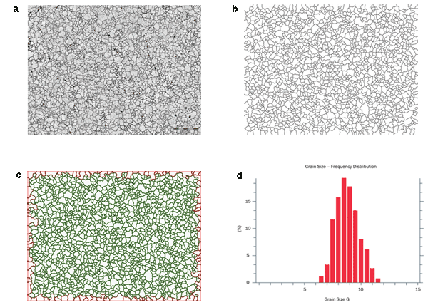
Grain-size determination of a special steel sample: (a) is the microscope image with 200× magnification, (b) is a reconstruction, (c) is a measurement, and (d) shows the results of the grain-sized distribution. Photo courtesy of Buderus Edelstahl GmbH of Wetzlar, Germany.
It helps to have widely varying magnification and capabilities in a single microscope, which Bauer said is why, a few years ago, Leica Microsystems introduced a device offering 7× total magnification and a 35-mm diameter field of view. With a switch of objectives, the same device also offers a 150× magnification with an i-line, or 365-nm ultraviolet light source, enabling a resolution of 140 nm. The target market for the system is semiconductor inspection, where surveying large areas at low magnification is beneficial but where users also need to discern very small features in selected regions of interest.
Looking forward, one trend should be increasing inspection and analysis automation, such as tools that classify steel based upon the nature and quality of inclusions. Removing people from the loop makes quality measurements more exact and repeatable. Carmakers and steel processors are two of the industries investing in this capability, Bauer noted.
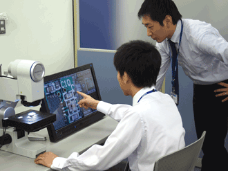
Other changes in the works for microscopes are the elimination of eyepieces and making systems easier to use by adding a dose of software. Japanese microscope maker Olympus, which has its U.S. headquarters in Center Valley, Pa., is one company moving toward optodigital systems. Two years ago, Olympus introduced a product line that got rid of the traditional eyepieces, replacing these with cameras and monitors. The change, along with software, brought some important benefits.

Microscopes are eliminating eyepieces in favor of cameras and monitors, allowing collaboration during inspection. Photo courtesy of Olympus.
“You don’t need to be an expert anymore to get a perfect image. Five, 10 years ago, you had to know what the sliders did and what the aperture stops did. What we’ve done now is to take it out of the hands of the expert and put it in the hands of anyone,” said David Rideout, director of sales and marketing for industrial microscopes at Olympus North America.
The system’s best image-function
capability examines the sample using nine different lighting and imaging techniques. These are presented to the user, who then selects the best combination. Importantly, this recipe can be fixed, eliminating human variability and thereby boosting inspection repeatability.
Putting images on a screen instead of looking through an eyepiece can be advantageous. For one thing, more than one person can view them at a time, which is vital during training or when collaborating. Another plus is that this approach can be less tiring, since operators can sit upright and shift their view.
One challenge: Inspection must handle smaller and smaller features, particularly in R&D or in manufacturing of advanced products. Resolution and measurement precision are tied to illumination wavelength, which means a push to shorter wavelengths. In the case of Olympus, this shows up in the company’s laser confocal microscopes, which use a 405-nm source. By using a wavelength on the edge of the ultraviolet, the systems can image and measure smaller features.

Phase analysis of a ferritic-perlitic: (a) is the microscope image, and (b) is a visualization of the different phases. Photo courtesy of Buderus Edelstahl GmbH of Wetzlar, Germany.
Light sources and illumination techniques can also provide other benefits. For instance, Olympus has a system that offers a combination of bright- and darkfield illumination, according to Rideout. It does so using two light sources to extract additional information from a sample.
In the future, there will be more systems and not just simple microscopes, Rideout predicted. This will increase use of software, as well as choices for system makers about what capabilities to include and what to exclude. Making the complex simple is also a challenge.
Microscopes are evolving in different directions, according to Darrell Sanderson, director of industrial sales at Nikon Metrology Inc. of Brighton, Mich. A subsidiary of its Japanese parent, Nikon Metrology offers a range of optical microscopes. Some provide noncontact 3-D measurement capability. For those instances where optical techniques aren’t sufficient, the company has a line of x-ray tools and has also partnered with scanning-electron-microscope maker JEOL.

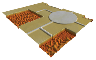
Mapping done with a 3-D optical microscope shows a pattern etched into a semiconductor wafer. Photo courtesy of Bruker Nano Surfaces.
As for the different evolution trajectories, systems intended for laboratory use tend to be flexible. In contrast, many microscopes used in industrial production applications are specialized tools dedicated to a specific task. Some are low magnification, such as those for deburring metallic parts and other manual operations. Others offer automated inspection, steadily scanning a sample in both X and Y directions until an entire area is covered. High magnification creates a shallow depth of field, and moving the focus up and down can yield 3-D information.
“In some cases, we can automate it and we can offer motorized stages for control,” Sanderson said. “In the case of a vision system, we can even add a touch probe, where we have something that can contact the part that is not visible and relate that data point to other features that are observed noncontact.”
One driving factor behind microscope developments is the need to do quality control and quality assurance. Another is the requirement to meet legislative and regulatory mandates. A third is the necessity to deal with finer and finer features.
A recent trend has been a switch away from traditional tungsten and halogen illumination to LED light sources, Sanderson said. Two advantages: LEDs last longer and don’t produce as much heat. A disadvantage is that the color temperature of LEDs differs from traditional sources, which means that some retraining of microscope users may be needed. Samples may not look the same, particularly in terms of color, when viewed using the new illumination technology.
Similarly, some user adjustments may be needed as monitors replace eyepieces. This transition is under way, although image-capture and display technologies still need to improve somewhat, according to Sanderson.
Some features are just too small for inspection with a standard microscope. Possible solutions involve the use of shorter wavelength sources, optical techniques based on interferometry or light scattering, or the use of electron microscopy. Technologies like Nikon’s perfect focus, which automatically corrects for sample or system thermal drift or vibration, can extend the capabilities of light-based microscopes.
Finally, it’s important to remember that the world isn’t flat. That’s why Tucson-based Bruker Nano Surfaces, a subsidiary of its German parent, supplies 3-D optical microscope systems, atomic force microscopes and stylus profilers. All offer high-accuracy 3-D images of an area of interest.
“We do it using interferometry,” said Matt Novak, director of technology and applications development. “We use specialized microscope objectives that split the light into two paths and then recombine a reference beam and a test sample beam. We look at the signal that’s created by the recombined light to map out the height of the surface.”
This noncontact method is aided by the use of high-brightness LEDs as a light source, Novak noted. The intensity of the source increases the signal, helping to overcome optical noise. All of the company’s systems use cameras and monitors instead of traditional eyepieces.
Bruker has debuted proprietary technology, AcuityXR, that offers lateral resolution below the traditional diffraction limit and three times better repeatability in lateral measurements than conventional systems. This is achieved through low-noise hardware and computational algorithms, Novak said.
As for trends, he pointed to increasing miniaturization, which shows up in consumer electronics and 3-D printing. The two areas could play a role in the rollout of the Internet of Things, with something like a predicted 50 billion connected devices due to appear within a decade in everything from toasters to tablets. Making that happen will require microscopy, in part because of the nature of all of those devices.
“They all require a lot of really small, intricate electronics designs,” Novak said.