Novel technology fills the gap between back-side-thinned and front-illuminated CCDs.
Behnam Rashidian, Dalsa Life Sciences
The demand for cost-effective, high-performance imaging detectors is prevalent within the scientific research community.
CCD sensors are arrays of photosensitive pixels that are covered by parallel layers of polysilicon gates. The layers provide a structure to store and transfer charges that are created in the pixels, which are fabricated on a silicon substrate that forms the back side of the CCD. In a front-illuminated CCD, the incident photons pass through the gates. In a back-illuminated or back-side-thinned CCD, the incident light passes through the thinned silicon substrate of the sensor. Because the attenuation of polygates is eliminated, back-side-thinned sensors provide much higher light sensitivity.
CCD sensors are used widely in life sciences, medical x-ray and scientific imaging applications, which demand higher image quality from sensors at lower incident light intensities, when compared with conventional applications such as industrial imaging.
Quantum efficiency — the number of electron-hole pairs generated per incident photon in a CCD sensor — plays a vital role in x-ray, life sciences and low-light scientific applications. Normally, the available light intensity in these applications is very low, as in the case of bioluminescence imaging, or must be minimized, as in the case of medical x-ray imaging.
Higher quantum efficiency translates into higher detector sensitivity, superior image quality and lower acquisition times. In terms of x-ray applications, higher quantum efficiency in a detector translates into lower patient exposure to x-ray radiation.
Whereas many different techniques are employed to increase the available light intensity in various medical and scientific applications, technologies employed in sensors to use available light intensity efficiently are equally important.
Higher quantum efficiency
For example, in a CCD x-ray detector (consisting of an x-ray-to-visible photon conversion layer and a CCD sensor), higher scintillation efficiency of the conversion layer results in a higher number of generated visible photons per incident x-ray quanta. The higher scintillation efficiency translates into higher quantum efficiency of the detector. However, on the sensor side, the quantum efficiency of the detector is affected directly by that of the CCD sensor also. Therefore, in CCD x-ray detectors, the combination of the scintillator material and the CCD quantum efficiency must be optimized for the highest achievable detective quantum efficiency.
Imaging dye-labeled cells using a CCD camera is another example of a scientific imaging application that can benefit from CCDs with higher quantum efficiency. In drug discovery applications, CCD cameras commonly are used to observe low-intensity light emissions that indicate the level of drug interaction with the biological subject. Higher quantum efficiency in such applications translates into higher signal-to-noise ratios, shorter acquisition times and smaller fluorescent sample amounts.
Comparison of technologies
Figure 1 depicts typical CCD quantum efficiency curves using various fabrication technologies available from Dalsa Corp. of Waterloo, Ontario, Canada. The conventional CCDs used in many industrial applications have quantum efficiency curves that peak at about 30 percent (green curve). The company’s standard technology (ST) is used to fabricate this type of sensor.
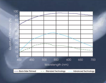
Figure 1. There is a sizable gap between the scientific-grade front-illuminated CCD (blue) and back-illuminated CCD quantum efficiencies (black).
The blue curve represents the quantum efficiency of Dalsa’s advanced technology (AT), which uses a thin polysilicon gate structure. These gates have better photon transmission efficiency than the standard thick polygates used in ST, resulting in better quantum efficiency of the sensor. The quantum efficiency curve of these sensors peaks at about 55 percent, making them suitable for many low-light imaging applications as well as for medical x-ray applications.
Although scientific-grade front-illuminated CCDs used in AT provide quantum efficiencies as high as 55 percent, the next step toward higher quantum efficiency has been to use more expensive and complex detectors based on the back-side-thinned CCD technology. As illustrated in Figure 1, quantum efficiency curves that peak at ~95 percent could be achieved using this technology. Back-side-thinned sensors provide excellent quantum efficiency in a broad range of wavelengths.
There remains a big performance gap between front-illuminated and back-side-thinned sensors. Dalsa’s High Quanta technology provides higher quantum efficiency (peaking at ~80 percent) in a front-illuminated CCD sensor than that found in conventional front-illuminated CCDs, while avoiding the complexity and cost of the alternative back-side-thinned sensors. This technology bridges the gap indicated above and provides a cost-effective alternative for applications that demand higher detector sensitivity and image quality.
High Quanta sensors are fabricated on a p substrate and potentially can be back-side-thinned as well. This provides an option to camera designers to reuse the same platform for both types of sensors as well as easy future upgrades for end users.
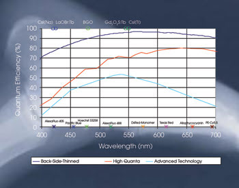
Figure 2. Shown are the quantum efficiency of sensors based on High Quanta technology as well as the peak wavelengths of commonly used scintillators and fluorochromes.
As seen in Figure 2, the quantum efficiency curve of the High Quanta CCD falls between the AT and the back-side-thinned sensors, thus filling the gap. The benefit compared with AT is more apparent at wavelengths from 550 to 700 nm.
Additional benefits
Also in Figure 2, the peak emission wavelengths of common scintillator materials used in medical x-ray imaging are marked on top. On the bottom, the peak emission wavelength of fluorochromes commonly used in fluorescence microscopy and in flow cytometry that range from 400 to 700 nm also are marked.
Two common scintillator materials used in medical imaging are thalli-um-doped cesium iodide and Gadox (Gd2O2S:Tb) with peak emission of about 550 nm. The quantum efficiency of High Quanta at this wavelength is about 71 percent compared with 54 percent from AT — about 30 percent higher; therefore, we expect higher detective quantum efficiency in sensors because of this gain.
Another example is the detection of fluorescence from fluorochromes with peak emission wavelengths of 500 to 700 nm. The difference in the sensor quantum efficiency between the High Quanta and the back-side-thinned technology at these wavelengths is minimal.
Meet the author
Behnam Rashidian is senior product manager at Dalsa Life Sciences in Waterloo, Ontario, Canada. He is responsible for managing all phases of product planning, development, marketing and sales as well as execution throughout the product life cycle; e-mail: [email protected].