Researchers from Nanjing University have proposed an active-passive photonic integration scheme that showcases a photonic integrated circuit chip that combines a light source, modulator, photodiode, waveguide, and Y-branch splitter, all based on a gallium-nitride (GaN)-on-silicon platform. What sets this approach apart, according to its developers, is that all active devices, including the light source, modulator, and photodiode, are built on the same ultraviolet InGaN/AlGaN multiple quantum-well (MQW) structure. This significantly reduces fabrication complexity and cost, they said.
InP-based photonic integration is recognized as a reliable and comprehensive active-passive platform, though it has limitations in terms of yield and substrate size. Monolithic silicon photonics, on the other hand, boast excellent passive performance, temperature-intensive modulators, and compatibility with complementary metal oxide semiconductor (CMOS) fabrication. Yet, the lack of a light source has so far hindered the development of this technology.
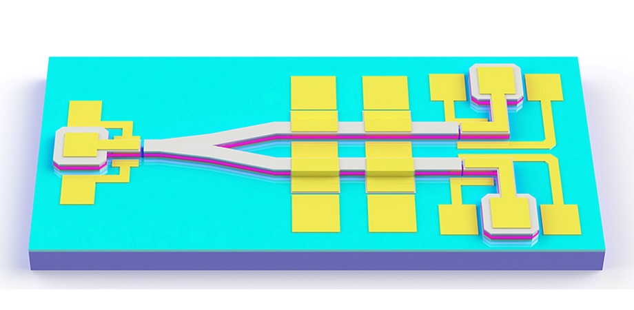
Photonic integration with active-passive functions based on GaN-on-silicon platform. Courtesy of Jiabin Yan, Nanjing University of Posts and Telecommunications.
The researchers designed their circuit chip based on the GaN-on-silicon platform and using III-nitride epitaxial layers grown through metal organic chemical vapor deposition. The monolithic, top-down approach builds III-nitride transmitters, modulators, waveguides, beamsplitters, receivers, and monitors on a conventional GaN-on-silicon wafer and does not involve regrowth or postgrowth doping.
The researchers characterized the resulting chip extensively from various perspectives to validate the effectiveness of this innovative photonic integration scheme. Results indicated that a higher reverse bias voltage applied to the modulator led to increased light absorption, as caused by changes in the absorption coefficient. The distinctive modulation effect was reflected in the receiver’s photocurrent changes. The test system demonstrated negligible cross-talk and the isolation between the light source and modulator on the same waveguide, achieved through p-contact layer separation, proved sufficient for optimal system performance.
By employing direct and indirect modulations within a single light path, the researchers simultaneously transmitted two types of data or encrypted one modulation signal’s data transmission with another modulation.
The researchers’ results further validated the data transmission and processing using UV light with a peak emission wavelength of 386 nm, the researchers said. In addition, “The adoption of multifunction MQW completely overcomes the compatibility problem of different optical active devices and considerably reduces fabrication complexity,” they said.
According to research team leader and senior corresponding author Yongjin Wang of the Peter Grünberg Research Center at Nanjing University of Posts and Telecommunications, further advancements in III-nitride etching accuracy added to the proposed integration scheme hold high potential for next-generation photonic integration. Applications in the sensing field, where high integration density is not a critical requirement, Wang said, are especially promising.
The research was published in Advanced Photonics Nexus (www.doi.org/10.1117/1.APN.2.4.046003).