Francesca Moglia, European Photonics Industry Consortium (EPIC)
Over the past few years, the boom in additive manufacturing of nonmetallic materials has been driven both by a large variety of applications, ranging from biomedicine to optoelectronics, and by the various technologies that sustain them. The growing potential for innovation means it is a good time to look at the developments in this arena by companies of different sizes and longevities.
In additive manufacturing, two-photon polymerization (TPP) is a technology that can generate high resolution and throughput. TPP is a direct laser writing technology in which the light-matter interaction takes place only within the volume of a focused laser spot. Here, the simultaneous absorption of two photons triggers the locally confined polymerization of an exposed photo-
resist. The laser focus can then be moved through the volume of the photoresist along all three spatial dimensions, and complex 3D structures are written along the laser’s trajectory.
With the TPP process, very complex structures can be fabricated in one step, without the need for subsequent deposition of fresh material. Nonlinear absorption enables a resolution below the diffraction limit, as opposed to conventional laser-based 3D printing technologies that only function within that limit. At the same time, the TPP technology is scalable, and very accurate submicro-meter resolutions can be combined into centimeter-scaled final products.
One company that is devoted to the development of maskless 3D lithography equipment based on TPP is Multiphoton Optics GmbH. Its modulator LithoProf3D-GSII equipment supports the manufacturing of optical packages, photonic components, and biomedical and life science products. The company supplies a process that automates high-precision optoelectronics assembly and allows interconnecting optical components, silicon or III-V photonic chips, and the creation of novel optical component packages that can also be used for co-packaging.
The applications range from hardware for big data computing and storage systems to optical transport infrastructure. The technology can offer low surface roughness (down to 5 nm for endoscopic objective lens systems), long-term stability (above 20,000 working hours), and broad options in scalability (Figure 1).
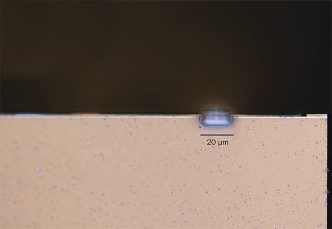
Figure 1. A microlens printed directly on the laser facet. On-device printing via
two-photon polymerization allows for further miniaturization of components.
Courtesy of Multiphoton Optics GmbH, in cooperation with nanoplus Nanosystems
and Technologies GmbH.
Recently, Heidelberg Instruments Mikrotechnik GmbH — experts in high-precision photolithography and nanofabrication tools — acquired Multiphoton Optics, the goal of which is to combine and strengthen the expertise of both companies in the field of microstructures production.
Nanoscribe is developing solutions based on TPP in its new headquarters in the ZEISS Innovation Hub at the Karlsruhe Institute of Technology. The company offers hardware and software, tailor-made printing materials, and application-specific solutions for prototyping, mastering, and serial production. Nanoscribe works with its customers and external partners to tailor its products to the demands of actual industrial processes. One result is the maskless lithography system Quantum X, for which the company was honored with the Innovation Award at LASER World of PHOTONICS in 2019 (Figure 2).
Figure 2. Nanoscribe’s maskless lithography system, Quantum X, is based on Two-Photon Grayscale
Lithography. Courtesy of Nanoscribe.
The Two-Photon Grayscale Lithography system is designed to combine the performance of grayscale lithography with the precision and flexibility of Nanoscribe’s TPP technology, allowing ultraprecise control of structures and their surfaces by voxel tuning. The microfabrication technology redefines the design scope for flat optics, such as refractive or diffractive micro-optics for industrial applications. Diffractive optical elements (DOEs) — with up to 256 discrete or quasi-continuous levels —
angled surfaces, freeform lenses, densely or randomly packed microlens arrays, high-aspect-ratio structures, and topographies with a surface roughness of <10 nm without post-processing are all achievable with stable processes. Nanoscribe systems are capable of precisely printing complex optical structures on photonic integrated circuits, optical fiber tips, and premanufactured wafers (Figure 3).
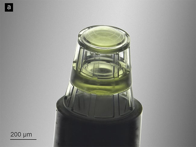
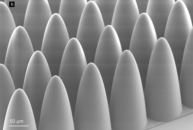
Figure 3. A compound microlens with diffractive structures 3D-printed on an optical fiber (a). Courtesy of TTI GmbH TGU Printoptics. A microlens array with high aspect ratios and a sag height of 250 µm (b). Courtesy of Nanoscribe.
Another method for precise additive manufacturing is based on atomic layer deposition (ALD). The principle behind this method is that the surface is subjected to a first precursor gas, which adsorbs on the surface. Afterward, the excess first precursor gas is evacuated, and — after full evacuation of the excess — the second precursor gas is introduced, completing the reaction on the surface. In general, ALD relies on two or more reactions to control the deposition process. The method can be operated in two manners: spatial or temporal. Spatial ALD separates the different gases in space, whereas temporal ALD separates the gases in time. Independently of whether spatial or temporal is used, providing three-dimensional structures is not possible. A three-dimensional structuring system is therefore needed that provides high-resolution nanoscale 3D structures.
An innovative approach to reaching the third dimension is supported by the company ATLANT 3D Nanosystems. Its Nanofabricator is an atomic-layer 3D printer that combines a direct-write ALD technique — due to confined-surface chemical reactions — with microfluidic systems, AI process monitoring and optimization, and precision mechanics. The device does not require a cleanroom and can be employed for the production of advanced electronic material and micro- and optoelectronics. It is able to implement 450 different high-purity materials and combine them with atomic-layer precision. With this machine, both rapid prototyping and manufacturing of micro- and nanodevices is possible.
The company’s μSADALP (Microreactor Selective Area Direct Atomic Layer Processing/Printing) technology provides for highly conformal, direct material deposition and removal with atomic precision. The μSADALP process works with reactive gases that create self-controlled, confined-surface chemical reactions — repeated in cycles — and allows the development, patterning, and multidimensional structuring of selected materials and devices. As a first priority, ATLANT 3D Nanosystems plans to approach the markets of advanced materials, MEMS, and sensors. Its technology has no significant limitation to working at zero gravity, and therefore it opens opportunities for in-space micro- and optoelectronics manufacturing.
Two companies in the market, with different technological strategies, are Hummink and Photosynthetic.
Hummink, created in 2020 and spun off from the physics laboratories of Pierre-Gilles de Gennes Institute (IPGG) and Ecole Normale Supérieure in Paris, uses a process that combines a nanometric “pen” with an oscillating macroresonator to perform capillary depositions of any liquid.
The system’s movement adapts to the specificities coming from either the ink (the viscosity) or the substrate (the topography), thanks to a closed-loop electronics setup inspired by atomic force microscope systems — thus enabling it to be material-agnostic. This process is only limited by common-sense physical limits: rheology, particle size, and surface energy. It offers a wide range of perspectives because the diameter of the nanopipette’s tip hole is adapted to the particle size and the desired deposition resolution.
This additive manufacturing technology enables the direct deposition of any liquid material — sols, gels, polymers, colloidal suspension of metal, protein, etc. — on any surface, with a high freedom of design and a resolution between 50 nm and tens of microns. Such performance can be secured on macroscopic-scale surfaces, from millimeters to tens of centimeters.
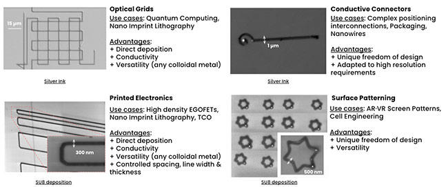
Figure 4. Examples of samples built by Hummink. SU-8: an epoxy-based negative photoresist; EGOFET: electrolyte-gated organic field-effect transistor; TCO: transparent and conductive oxide. Courtesy of Hummink.
Photosynthetic is basing its technology on a cheaper alternative to TPP — single-photon polymerization — exploiting advanced computational methods to achieve resolutions similar to the TPP approach. The goal is to create a polymer-based 3D printer capable of generating larger volumes of 3D structures with submicron resolution at unprecedented speed, on the order of 1 mm3/min, for rapid prototyping and fabrication of micro-optics, microfluidics, microsensors, and other microscale applications. The team at Photosynthetic is currently working on its first demonstration prototype.
Meet the author
Francesca Moglia, Ph.D., is a project leader at the European Photonics Industry Consortium (EPIC). She has a background in crystal growth, spectroscopy, optics, and laser development for research and large research facilities. Before joining EPIC, she moved from R&D to scientific management, to coordinate a consortium of funding agencies in the field of astroparticle physics. She graduated with a degree in physics from the University of Pisa in Italy, acquired her doctorate in the field of laser physics at the Universität Hamburg in Germany, and pursued her postdoctoral activities at Deutsches Elektronen-Synchrotron (DESY) in Hamburg.