
Advanced Imaging for Quantum Materials Research
As quantum research advances, ion traps, carbon nanotubes, and highly specialized cameras each play integral roles in the characterization of materials suitable for use as qubits.
By Michael Melle
Quantum theory seeks to explain the nature and behavior of matter and energy at the atomic and subatomic levels. Such phenomena are elucidated
via research that aims to manipulate the state of this matter and energy to achieve accurate, measurable, and repeatable results.
Modern quantum activity is very broad, encompassing both near-term commercial applications and long-term theoretical challenges. The “first wave” of quantum technology has been defined primarily as the discovery of quantum mechanics and principles of wave-particle duality. The “second wave” is based on the application of fundamental quantum principles such as superposition and entanglement to create highly practical new quantum technology, including exponentially faster computational methods and ultrasecure communications.
The analog to a classical bit (0 or 1) in the quantum world is the qubit. In a quantum computer, two qubits can represent four states (00, 01, 10, or 11) simultaneously, a fundamental principle of quantum mechanics known as quantum superposition. Another fundamental principle of quantum mechanics is quantum entanglement, in which the quantum states of multiple objects are described
in reference to each other, even if they are spatially separated.
The requirements for a quantum system, which is a collection of qubits, include the ability to initialize a well-defined quantum state, the availability and control of sufficient operations to launch the initial state to an arbitrary entangled state, and the ability to perform measurements of the qubits with high quantum efficiency1.
The creation of a qubit requires an object, such as a single photon or atom, capable of achieving a state of quantum superposition between two states. A significant amount of research is dedicated to the manipulation and characterization of materials suitable for use as qubits. Among the leading technologies used to manipulate and characterize such materials are atom/ion traps, neutral atoms,
superconductors/semiconductors, photonic systems, carbon nanotubes, quantum dots, and nitrogen vacancy (NV) centers in diamonds.
Additionally, advanced imaging technologies are integral to the characterization necessary for qubit materials study, and, ultimately, they aid advancements in quantum research and applications.
Trapped ions
Ion traps enable the manipulation and interrogation of atomic or molecular ions. By using a combination of electric or magnetic fields, charged particles are
captured in isolation. Such trapped ions can be controlled very well and are excellent quantum memories, providing single-qubit coherence in excess of 10 minutes (Figure 1).
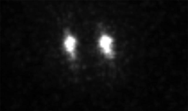
Figure 1. Individual trapped ions acquired with an electron-multiplying intensified CCD (emICCD) camera. Courtesy of Ferdinand Schmidt-Kaler, Kilian Singer, Johannes Rossnagel, and Georg Jacob/Institute of Physics, Mainz University.
Today’s ion traps have been developed not only to ensure that a sample is trapped but to obtain additional information, including the size and shape of the ion sample, the number of stored particles, their temperature, and the quantum state of the ions.
Detection of trapped ions necessitates amplification and imaging techniques that rely either on the light emitted by the ions or on their physical presence in the trapping electromagnetic field. Various detectors can be used to record light from the trapped ions, with charge-coupled devices (CCDs) providing an increasingly popular alternative to avalanche photodiodes (APDs) and photomultiplier tubes (PMTs) for imaging the emitted photons.
Ion states can be read with low error rates by collecting the emitted light using sensitive, high-resolution CCD cameras. These scientific detectors, which are
employed to acquire information about the spatial distribution of the trapped ions, are either coupled to an external image intensifier or they utilize an on-chip amplifier to boost the signal emitted by individual ions.
The first approach uses a gateable intensified CCD (ICCD) camera whose CCD is fiber-optically bonded to an image intensifier that features one of several Generation 2 or 3 photocathodes designed for ultraviolet, visible, and/or near-infrared wavelength sensitivity. The second approach utilizes a nongateable electron-multiplying CCD (EMCCD) camera, which adds supplementary
“electron multiplying” gain to the detection process via impact ionization and delivers excellent system linearity.
A class of newer cameras (emICCDs) combines these two technologies, offering the abilities to synchronize the camera with well-defined trigger events, such as laser pulses, to provide gating times in the picosecond range and to maintain high linearity (Figure 1)2.
Cold atoms
A Bose-Einstein condensate (BEC) is a state of matter of a diffuse gas of bosons cooled to temperatures very near absolute zero. All the atoms of a BEC are in a highly coherent quantum state, one in which there is quantum entanglement among the constituent atoms. In 1995, Eric A. Cornell and Carl E. Wieman of the Joint Institute for Lab Astrophysics
(JILA) in Boulder, Colo., as well as Wolfgang Ketterle of the Massachusetts Institute of Technology (MIT), became the first researchers to create BECs. The three were awarded the Nobel Prize in physics in 20013.
The motion, shape, and forces between cold atoms can be efficiently controlled. Most experiments for cold atoms involve optical observations (Figure 2)3 that utilize some form of probe laser scattering. Fluorescence imaging detects re-emitted photons, absorption imaging detects the shadow of atomic absorption, and phase contrast imaging detects shifting in the phase of the unscattered light.
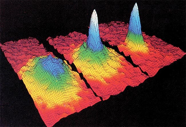
Figure 2. Successive occurrence of Bose-Einstein condensation in rubidium. (Left to right) The atomic distribution in the cloud just prior to condensation, at the start of condensation, and after full condensation. High peaks correspond to a large number of atoms. Silhouettes of the expanding atom cloud were recorded
6 ms after switching off the confining forces of the atom trap. Courtesy of Royal Swedish Academy of Sciences/www.nobelprize.org.
State-of-the-art EMCCD cameras, which can incorporate an on-chip mask that allows more than 1 million frames per second to be captured when operated in kinetics mode, are ideally suited for BEC observations.
Single photons
Another example of a quantum particle that can be used as a qubit is a photon. Photons offer the ability to increase the number of states — such as polarization, frequency, time, and location — all
without increasing the number of photons4.
Accurate detection of single photons requires the use of extremely sensitive instruments, such as scientific CCDs, ICCDs, EMCCDs, emICCDs, or new scientific complementary metal-oxide-semiconductor (sCMOS) cameras with high-quantum-efficiency (QE), back-illuminated architectures.
Single-photon detection and single-photon spectroscopy are important emergent techniques. Dark-state, bright-state, and superposition-state data can be
derived from the photon-counting capabilities of an advanced ICCD camera5 (Figure 3).
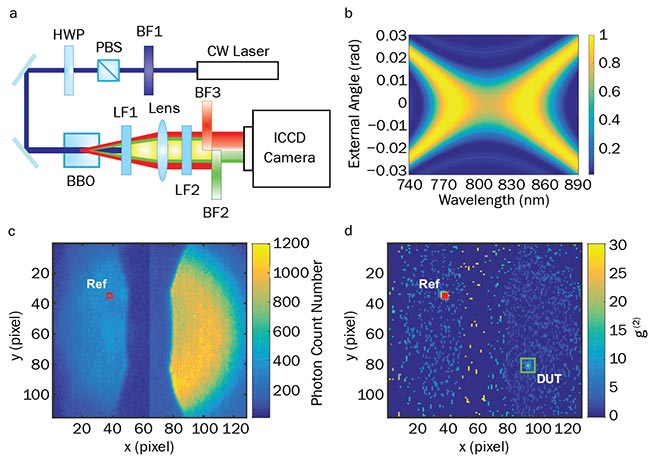
Figure 3. Autonomous absolute calibration of an ICCD camera. Experimental setup (a). Calculated wavelength-angular spectrum for collinear slightly nondegenerate SPDC (spontaneous parametric down-conversion) (b). Typical image taken with an ICCD camera by acquiring 4.8 million frames (c). Pixels inside red square chosen as ‘reference’ detector. Result of second-order normalized intensity correlation function g(2) measurement between reference detector and all other pixels of camera (d). Filled red square marks reference detector (same as in panel c). Empty green square shows chosen DUT (device under test). BBO: Beta barium borate; BF: bandpass filter; LPF: longpass filter; PBS: polarizing beamsplitter; HWP: half-wave plate. Courtesy of Optical Society of America (OSA).
Diamond NV centers
A nitrogen vacancy (NV) center is a defect formed in diamond by one substitutional nitrogen atom and an adjacent vacancy. They can be controlled coherently using electromagnetic fields at room temperature. NV fluorescence allows simple routes for optical initialization
and readout.
NV centers have good coherence times (>1 s) and possess exceptional light-to-spin properties for exploitation in quantum information and entangled photon sources. Applications include quantum computing, medical imaging, and nanoscale sensing.
Figure 4 shows a recent experimental setup for NV center imaging along with resultant data6. Synchronization of a microwave generator, an acousto-optical modulator (AOM), and an emICCD camera is achieved by operating the camera in its external trigger mode and counting the number of frames output by “logic out.” Contrary to a detection setup that combines a boxcar with a PMT, the fast gating and excellent on/off ratio of the quantitative, ultrahigh-sensitivity emICCD camera yields a measurement that is insensitive to the first laser initialization pulse.
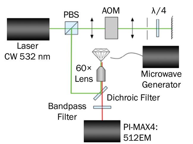
Figure 4. Laser pulses are generated by the acousto-optical modulator (AOM) in a double-pass configuration and sent to the sample with a polarizing beamsplitter (PBS). The detector used is an emICCD camera. Rabi oscillations of an NV (nitrogen vacancy) ensemble on an individual pixel (blue) and 10- × 10-pixel region (red) are shown; inset describes pulse sequence for the laser initialization (I) and readout (R) of the NV centers. Microwave (MW) pulses are applied between the laser pulses. Courtesy of David Roy-Guay/Université de Sherbrooke.
Quantum dots
Quantum dots are tiny particles or nanocrystals of a semiconducting material with diameters ranging from 2 to 10 nm (10 to 50 atoms). Currently used in medicine, photovoltaics, displays, and biosensing, quantum dots have features that could also be useful in quantum information processing.
Lead sulfide (PbS) quantum dots, for example, are an important semiconductor material that provides potential for applications such as telecommunications, tunable IR lasers, and solar cells. The
first single-nanocrystal spectral study for PbS quantum dots emitting in the shortwave-IR (SWIR) region at ~1250 nm was reported recently (Figure 5)7.
The image was captured by a liquid-nitrogen-cooled InGaAs (indium gallium arsenide) focal plane array (FPA) camera coupled to a high-precision imaging
spectrograph with a 320-mm focal
length.
Figure 5. Image of a region of a concentrated PbS (lead sulfide) quantum dots sample taken using a 2D InGaAs (indium gallium arsenide) detection array capable of being cryogenically cooled down to -190 °C coupled to an imaging spectrograph. (Excitation: CW 405 nm. Power density: 3 W/mm2. Integration time: 10 s. Objective: 50×/0.65 NA. Room temperature.) Courtesy of Han Htoon/Materials Physics and Applications Division of the Center for Integrated Nanotechnologies.
This cryogenically cooled InGaAs camera’s unprecedented long integration times and low dark counts enabled the groundbreaking single-nanocrystal spectral experiments mentioned above by providing levels of contrast and sensitivity that cannot be achieved with other InGaAs cameras when working with PbS quantum dots.
It is noteworthy that the same type of high-performance InGaAs camera has also been used by a research group at MIT to evaluate novel InAs (indium arsenide)-based SWIR quantum dots. The researchers were able to demonstrate that these new SWIR-emitting core/shell quantum dots hold tremendous promise for the next generation of in vivo SWIR imaging8,9.
Carbon nanotubes
Among the myriad potential applications of carbon nanotubes are optical-based quantum cryptography and quantum computing. As with the latest quantum dot research, investigations of carbon nanotubes are now benefitting from the superb SWIR sensitivity and long integration times afforded by highly advanced, cryogenically cooled InGaAs FPA cameras.
Several studies are focusing on the development and photophysical probing of carbon nanotube defect states as routes to room-temperature, single-photon emitters at telecom wavelengths (Figure 6)10,11.
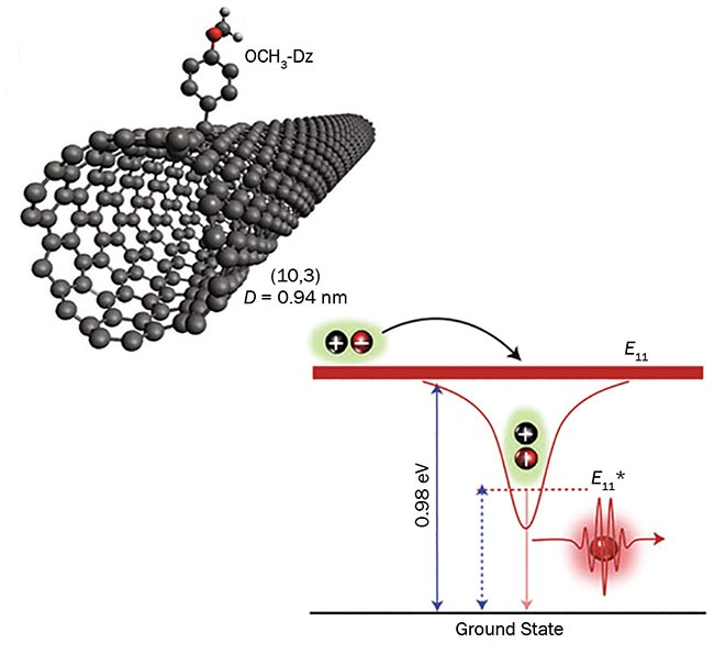
Figure 6. Depiction of a carbon nanotube defect site generated by functionalization of a nanotube with a simple organic molecule. Altering the electronic structure at the defect enables room-temperature, single-photon emission at telecom wavelengths. Courtesy of Los Alamos National Laboratory.
As fundamental research into quantum materials continues to evolve, so too must the imaging technologies that facilitate such efforts. Given the ever-expanding complexities of this field, careful consideration is required when selecting the most effective and most appropriate solution for a specific imaging application or set of applications.
Critical factors in determining which advanced imaging technologies should be utilized for quantum materials research often include a camera’s ability to provide excellent quantum efficiency (QE) at
key wavelengths, high spatial resolution, flexible regions of interest, gating down
to the picosecond range, fast readout speeds, very low read noise and thermally generated noise, long exposure times,
reliable quantitative performance (linearity over a broad dynamic range), sufficient single-pixel full well, minimal clock-induced charge, full software compatibil-
ity, and seamless integration within an experiment.
Meet the author
Michael Melle is the imaging product manager for Teledyne Princeton Instruments. He
manages the business segment comprising x-ray, visible, and shortwave-IR cameras for scientific research, industrial imaging, and OEM communities. He has a B.S. in mechanical engineering from Lehigh University and
an extensive background in imaging and
computer vision for the scientific, industrial, and defense industries; email: mmelle@
princetoninstruments.com.
References
1. National Research Council (2007).
Controlling the Quantum World: The
Science of Atoms, Molecules, and Photons. Washington, D.C: The National Academies Press, https://doi.org/10.17226/11705.
2. Princeton Instruments Inc. (2015).
Application note: ultra-high-sensitivity emICCD cameras facilitate use of trapped ions for quantum research.
3. Nobel Media AB (2001). Information for
the public, www.nobelprize.org/prizes/physics/2001/popular-information/.
4. Optical Society of America (2019).
Researchers move closer to practical
photonic quantum computing, https://phys.org/news/2019-02-closer-photonic-quantum.html.
5. L. Qi et al. (2016). Autonomous absolute calibration of an ICCD camera in single-photon detection regime. Opt Express,
Vol. 24, Issue 23, pp. 26444-26453,
https://doi.org/10.1364/OE.24.026444.
6. Princeton Instruments Inc. (2015).
Application note: ultra-high-sensitivity emICCD cameras enable diamond quantum dynamics research.
7. Princeton Instruments Inc. (2018). Case study: measuring spectra of single quantum dot nanocrystals emitting in SWIR.
8. Bruns et al. (2017). Next-generation in vivo optical imaging with short-wave infrared quantum dots. Nat Biomed Eng 1, Article no. 0056.
9. Princeton Instruments Inc. (2018). Application note: deep-cooled InGaAs FPA camera enables high-speed, high-resolution in vivo imaging of SWIR-emitting quantum dots.
10. Los Alamos National Laboratory (2018). Carbon nanotube optics poised to provide pathway to optical-based quantum
cryptography and quantum computing, https://phys.org/news/2018-06-carbon-nanotube-optics-poised-pathway.html#jCp.
11. X. He et al. (2018). Carbon nanotubes as emerging quantum-light sources. Nat Mater, Vol. 17, pp. 663-670.
/Buyers-Guide/Teledyne-Princeton-Instruments/c12186