Semiconductor lasers coupled with beam-shaping optics are the engine driving continued development of more capable, compact, and cost-effective automotive lidar systems.
LEON LI, FOCUSLIGHT TECHNOLOGIES INC.
Lidar for autonomous
vehicles debuted in 2007 as an enabling sensor technology for robotaxis and robotruck development. Within the last five years, however, the technology has trended toward broader commercialization in mass-market passenger vehicles, as evidenced by a dozen volume contracts or project nominations signed by OEM carmakers and lidar providers. Mercedes-Benz, for example, announced in December 2021 that its first model to offer Level 3 autonomy will be equipped with lidar. The number of contracts will grow even faster in the next few years as lidar enables more passenger vehicles with Level 2 or Level 3 autonomy.
The technology’s accelerating commercialization underscores how far lidar has evolved beyond its earlier architecture, in which dozens of laser emitters and avalanched photodiodes were assembled onto a 360º rotating base. A number of innovative lidar architectures and sensor technologies have since been developed. Among the various architectures’ popular scanning methods are MEMS-based laser-spot 2D scanning, rotating mirror line-beam 1D steering, mixed 2D
mechanical scanning, and flash illumination without any scanning.
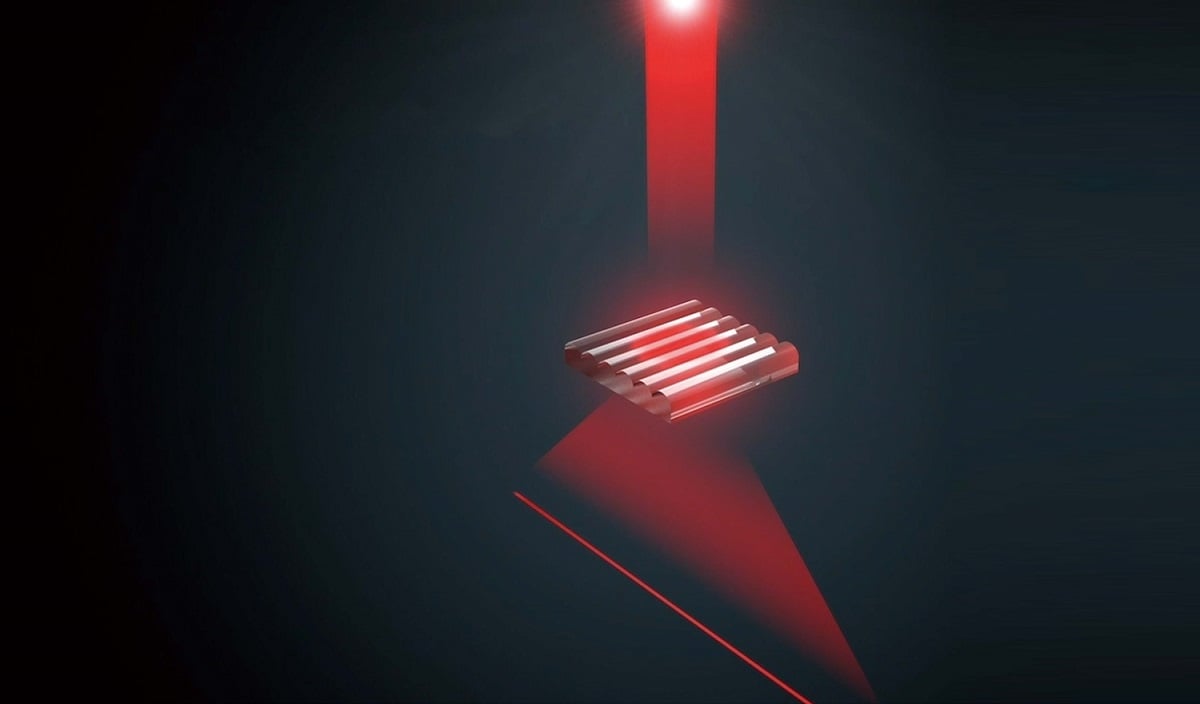
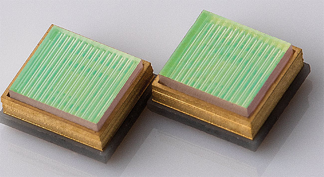
Line-beam-shaping optics for line-beam-steering lidar applications. Courtesy of Focuslight Technologies.
A unifying theme underlies this diversity of developing lidar technologies, which is that the continued commercialization of the technology calls for further development in laser technologies. More specifically, this call applies to the four laser types commonly used for automotive lidar systems. They are edge-emitting lasers (EELs), vertical-cavity surface-emitting lasers (VCSELs), diode-pumped solid-state lasers (DPSSLs), and pulsed fiber lasers.
Solid-state and fiber lasers offer relatively higher pulsed energy, eye-safe emissions in the shortwave IR range, and higher beam quality versus EELs and
VCSELs. But the latter two laser technologies also have their advantages.
Largely based on gallium arsenide (GaAs) compounds, EELs and VCSELs are semiconductor lasers that operate primarily at NIR wavelengths, such as 905 or 940 nm, and are well known for their superior conversion efficiency, simplicity, and compatibility with automotive standards, and for offering the most compact form factor versus other lidar sources. As a consequence, semiconductor laser technology occupies the highest market share in the automotive lidar market, with EEL taking the predominant share.
VCSELs, however, have become a growing alternative. Widely used in telecom and datacom transceivers, and more recently in consumer electronic devices for 3D sensing, VCSELs are now targeting the automotive lidar market. Manufacturers have developed multijunction VCSEL devices, with the latest devices incorporating up to five or six junctions that generate several-times-higher peak power densities to meet the demand for lidar systems.
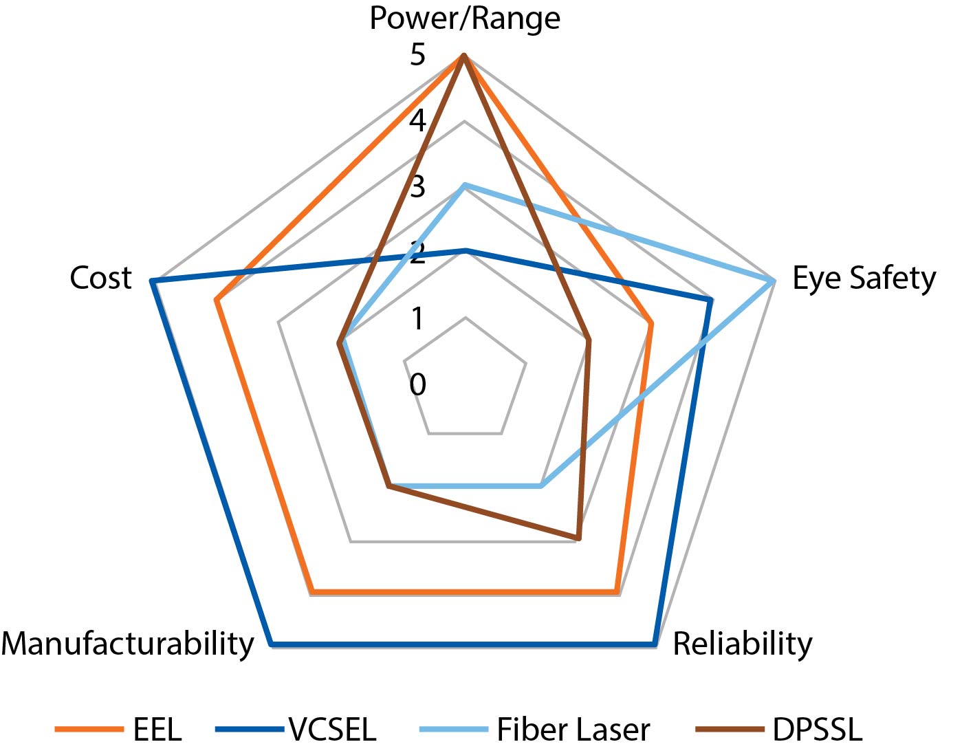
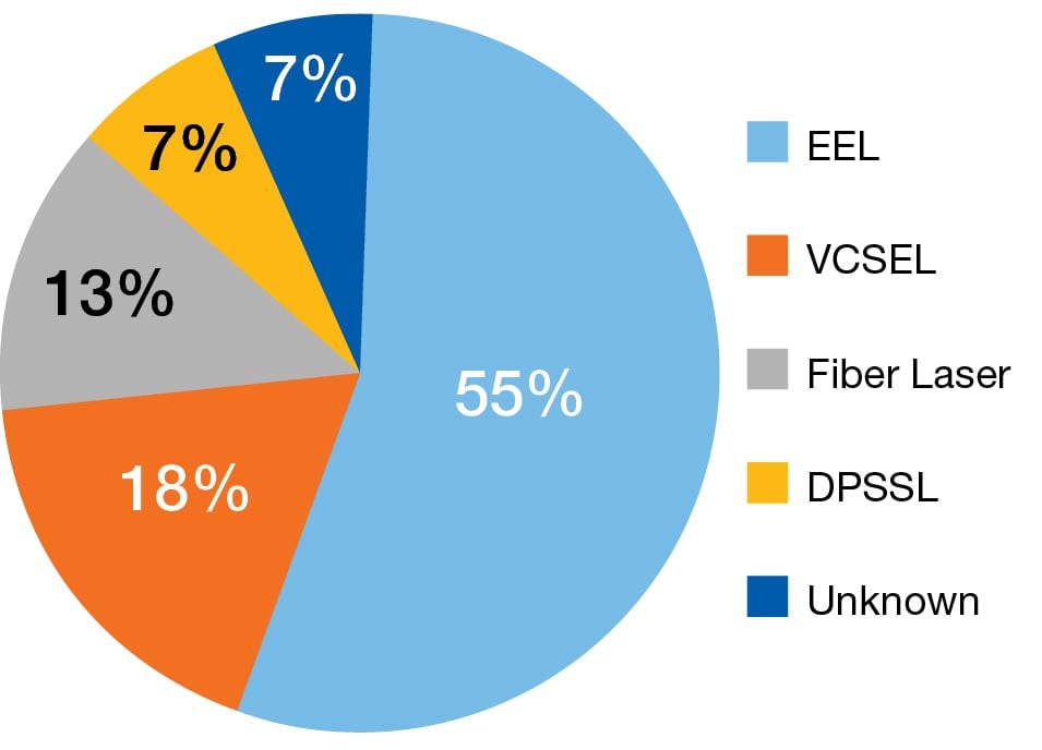
Automotive lidar systems typically leverage one of four laser types: edge-emitting lasers (EELs), vertical-cavity surface-emitting lasers (VCSELs), diode-pumped solid-state lasers (DPSSLs), and pulsed fiber lasers. Each has merits and drawbacks (top), and each has been adopted by lidar developers to varying degrees (bottom). Based on statistics compiled by Focuslight in a survey of over 50 lidar developers. Courtesy of Focuslight Technologies.
There are well-known pros and cons for VCSELs. While their power density per lasing area is an order of magnitude lower than EELs, they exhibit significantly lower wavelength temperature dependence and are less prone to facet damages, which translates into higher reliability. They allow easier implementation of two-dimensional emitter matrices with individually addressable rows and columns. This last advantage is significant enough to make VCSELs a preferred choice for solid-state flash lidar systems, as well as for their variation — sequential or segmented flash lidar for short- to mid-range detection at wide field of view (FOV). Ultimately, VCSEL technology could potentially become the most cost-effective option for high-volume production due to its efficient wafer-level coating, testing, and screening processes, as well as its compatibility with high-volume production.
Beam shaping
Despite their many merits, both VCSELs and EELs still face several challenges when applied in a lidar system. Semiconductor lasers are as famous for their poor beam quality as they are for their high optical efficiency.
A typical 10- × 200-µm nanostack EEL emitter with 120 W of nominal pulsed power has a typical beam divergence of 25° in the vertical axis and 10° in the horizontal axis, defined as full width half maximum (FWHM). The result is an elliptical beam pattern in the far field. In contrast, a typical VCSEL, regardless of its dimensions, usually has a symmetrical divergence around 25° on both axes, defined as FWHM.
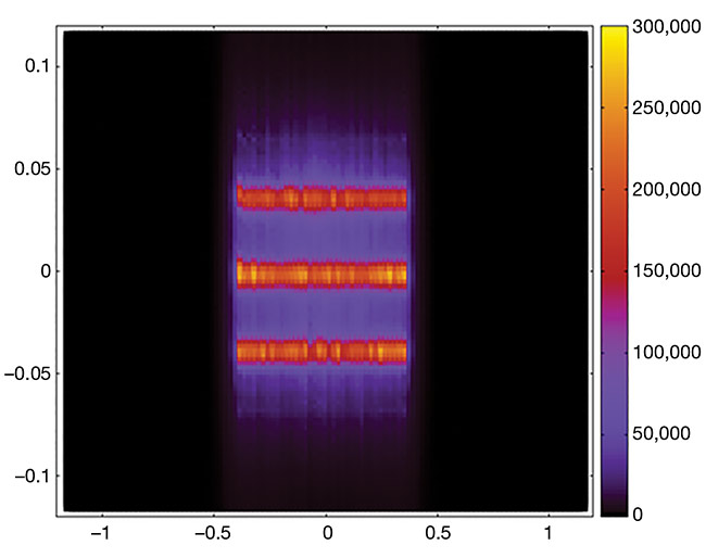

A typical EEL fast- and slow-axis collimator designed for use in MEMS lidar systems (top). Beam divergence for such systems (bottom) is typically 0.1° × 0.8° (middle). Courtesy of Focuslight Technologies.
These poor parameters make semiconductor lasers inadequate to be applied directly to mainstream lidar systems. Therefore, it is critical to ensure that they have a proper beam-shaping optical design that directs laser photons appropriately and transforms the original beam shape into the required beam patterns.
One common approach combines fast-axis and slow-axis collimation for the nanostack EELs used in MEMS-based lidar systems.
This combination requires careful design considerations to achieve the best possible collimation on both axes while at the same time restricting the beam size and making sure it is within the MEMS mirror’s clear aperture.
As lidar technology and architectures have evolved, two other advanced beam-shaping techniques have emerged for semiconductor lasers: the line-beam concept and the flash-illumination concept.
A line beam is usually generated by an EEL minibar fabricated as a linear array of nanostack EEL emitters. A line-beam-shaping design usually consists of a long-focal-length aspherical fast-axis collimation lens that generates horizontal divergence as small as <0.1° and a line-beam homogenizer that produces a typical and customizable 25° vertical divergence with high uniformity across its intensity distribution. Coupling these beam-
shaping techniques with a mechanical rotating mirror and a novel silicon photomultiplier (SiPM) or single-photon avalanche diode (SPAD) array on the detector end enables a new generation of hybrid solid-state high-resolution beam-steering lidar. To achieve such line-beam-shaping configurations, it is critical to generate a narrow, uniform, and clean-line laser beam with very low divergence in the fast axis, high uniformity, and minimum intensity outside the designed FOV.
The flash-illumination beam-shaping concept often utilizes two directional microlens arrays as diffusers in front of the VCSEL to generate a rectangular FOV with high uniformity or, in other cases, an FOV with specifically defined intensity profiles. Focuslight recently developed ultrawide-angle diffusers that can generate close to 160° FOV with a batwing intensity distribution, enabling ultrawide FOV for lidar or in-cabin sensing applications.
These beam-shaping concepts and solutions are advancing semiconductor laser applications for lidar by lowering system complexity and increasing system signal-to-noise ratios.
Advancements in the works
No perfect laser solution exists for lidar. However, laser and optics manufacturers are accelerating the pace of their innovations and research to address technical challenges and meet the fast-growing demand from the lidar market. Several potential advancements in semiconductor laser technology show promise.
For example, pulsed EELs are often packaged in a special quad flat no-lead (QFN) or transistor-outline (TO)-can configurations for automotive qualification and customer applications. Both laser package types present drawbacks, such as compromised thermal performance or higher parasitic inductance during short-pulse operation. An alternative approach under development is to bond the EEL die directly onto a driver printed circuit board (PCB) or a ceramic substrate for further packaging. EEL bare die bonding technology could provide an improved laser die packaging solution for lidar based on EEL minibars.
Another emerging advancement involves EELs with temperature-
dependence characteristics comparable to VCSELs.
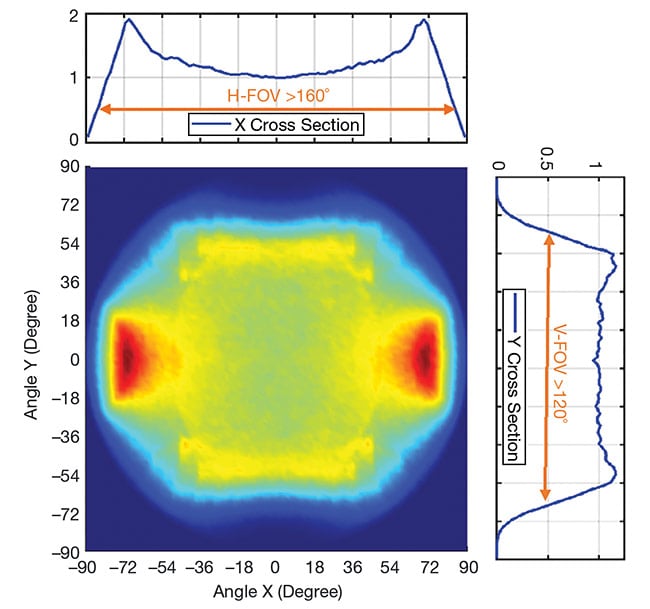
As lidar technology and architectures have evolved, advanced beam-shaping techniques have emerged for semiconductor lasers. The flash-illumination beam-shaping concept for VCSELs (top) utilizes two directional microlens arrays as diffusers in front of the VCSEL to generate a rectangular field of view (FOV) with high uniformity (bottom). Ultrawide-angle diffusers are a more recent development that can generate close to 160° FOV with a batwing intensity distribution, enabling wide-FOV lidar or in-cabin sensing applications. Courtesy of Focuslight Technologies.
Wavelength-stabilized EELs that share a comparable wavelength shift coefficient to VCSELs (e.g., 0.07 nm/ºC) could reduce the need for thermoelectric coolers for temperature control. They could also help narrow the spectral range of bandpass filters used on a lidar system’s receiver end to improve the system’s signal-to-noise ratio.
Semiconductor laser-makers are also tailoring their devices for lidar applications by adding more junctions to EEL and VCSEL architectures in a race to achieve higher peak powers. EELs have had the edge, so to speak. But VCSEL technology is catching up, with the development of devices incorporating up to eight junctions. EELs with four or five junctions are also being developed and tested in labs. Unlike VCSELs, EELs with more junctions offer an increased active emission area, which increases the challenges for beam shaping. Semiconductor laser designs with more laser junctions are attractive to lidar developers because laser slope efficiency and peak power density both increase proportionally with the number of junctions. Importantly, adding junctions also brings more challenges with regard to thermal design, manufacturing yield, and long-term reliability. Therefore, thorough qualification of these lasers must be completed before they can be used in commercial lidar systems.
Another potential breakthrough involves back-emitting VCSEL designs. Such devices would allow VCSEL production to leverage surface-mount technology, which would reduce the wire bonding and parasitic inductance that is common to VCSEL packaging and allow faster rise and fall times and shorter laser pulses. Back-emitting VCSELs also enable micro-optics to be etched on the GaAs wafers directly. This could be
a potential game changer because it
could enhance optical performance and significantly reduce lidar system complexity.
Semiconductor laser-makers are also developing devices that emit at eye-safe
SWIR wavelengths between 1340 and 1550 nm. NIR wavelengths such as 905 or 940 nm, at which semiconductor lasers typically operate, are only eye safe under a specific upper limit of energy density and eye exposure. In contrast, the 1470- and 1550-nm wavelengths permit an upper limit of energy density that is several times higher. Recent development of indium phosphide (InP)-based EELs with multiple junctions aim to deliver higher peak powers within the SWIR range for automotive lidar applications. The latest devices to emerge exhibit more than 100 W of peak power from a 200-μm strip width, with a three-junction InP EEL lasing at 1550 nm — a significant advancement. Nevertheless, it is still far from the peak powers that can be generated by a 1.5-μm pulsed fiber laser, so it has not yet made semiconductor sources a primary choice for commercialized lidar operating at these wavelengths. Producing high-power VCSELs that operate at SWIR wavelengths has also been consistently more challenging. While some recent cases use SWIR VCSELs as the illumination source for SWIR sensing systems, these sources still do not offer a primary solution for lidar applications.
Road to mass production
A semiconductor laser-based lidar system or its components and subassemblies must pass four milestones to be compatible with automotive-grade mass-production applications.
First, the system must be designed to deliver automotive-grade performance. This means a semiconductor laser and its beam-shaping optics must collectively perform within target specifications over a wide operating temperature range per automotive grade. EEL beam pointing and directivity shifting under wide operating temperatures is one of the top challenges toward reaching this goal. And significant research and development on both opto- and thermal-mechanical designs of these systems is required to minimize the optical performance temperature dependence.
Second, semiconductor laser systems must be tested and qualified as capable of delivering automotive-grade reliability. Despite the readiness of discrete semiconductor lasers and optics, customized automotive-grade qualification of an integrated laser-optics assembly remains a top challenge for most lidar developers.
Automotive reliability qualification
plans typically begin with a design verification stage on a smaller sample size of a few dozen laser systems followed by a product-validation step that can last from six to as many as 12 months, based on a few hundred samples. Passing these stringent qualifications for durability under high-temperature operating conditions, for example — or withstanding high-humidity testing — requires careful attention to laser, optical, thermal, and mechanical designs to ensure that their finished assembly will achieve an adequate reliability margin. Robust mounting of optics and reliable adhesive joints are critical to surviving these tests.
The third milestone that laser assemblies confront is the construction of an automotive-grade high-volume manufacturing line with high-level process automation. For critical processes, automotive parts manufacturers apply a process capability index (Cpk) to measure and monitor the ability of a process to meet target specifications. Automotive-grade semiconductor laser assemblies are no different. They must have a Cpk value that meets automotive standards to ensure that continuously produced samples can either pass product verification qualifications with zero failures or be delivered to automotive customers with zero defects. A failure in any qualification test will lead to a failure in the automotive-grade qualification. Achieving a passing Cpk value is only possible by using a high level of process automation, especially for the high production volumes forecast for automotive lidar in the next few years.
The final milestone must put in place a stringent and well-established automotive-grade quality management process following the International Automotive Task Force’s 16949 standard to ensure zero defects for continuous high-volume production and deliveries. This process is nothing new for automotive parts suppliers. But implementing it could be quite a challenge for most laser and optics manufacturers serving industrial markets with low to moderate production volumes.
Scanning forward
As any laser or optical technology matures and moves closer to mass production, the final and ultimate challenge will involve cost. Lidar developers targeting the automotive market face cost challenges that have never been seen in the photonics industry.
Semiconductor lasers intrinsically offer the merits of high efficiency, high simplicity, and high-volume cost-efficiency, making them the top choice for automotive lidar developers. And the market share for these devices will continue to expand as lidar is further commercialized — especially as ongoing advancements continue to address current shortfalls in the technology.
Meet the author
Leon Li is deputy general manager of the Automotive Business Unit at Focuslight Technologies Inc. He previously served as team leader of international sales and later as head of Focuslight’s Open Package Diode Lasers product line before he led a dedicated team to develop technologies and products for the lidar market; email: [email protected].