A new fabrication method makes vertical external cavity surface-emitting lasers in the 2.X-µm range possible, combining high output power and precise tunability.
PETER HOLL AND MARCEL RATTUNDE, FRAUNHOFER INSTITUTE FOR APPLIED SOLID STATE PHYSICS
Recently, there has been growing demand for light sources in the near- to mid-infrared range with high output power in combination with good beam quality. This demand is driven by applications such as optical pumping Holmium:YAG lasers or optical parametrical oscillators, as well as satellite communication through the atmosphere and material processing of optically transparent materials. The vertical external cavity surface-emitting laser (VECSEL) fulfills this need and is suitable for numerous applications in the mid-IR range.
VECSELs are referred to as semiconductor disk lasers because of the similarities to the setup of solid-state disk lasers (Figure 1). They combine several advantages in one compact light source: a circular beam profile, high output power in the several-tens-of-watt range and the wavelength flexibility of a semiconductor gain material. Since the first demonstration in 19971, the use of different semiconductor material systems has enabled direct laser emission in a wide spectral range, from the visible to mid-infrared. This range can be further expanded by using nonlinear optical materials in the external cavity, allowing for laser emissions in the ultraviolet C (UVC) to the terahertz regime.
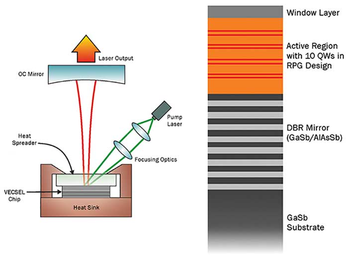
Figure 1. Schematic of a basic VECSEL setup with an intracavity heatspreader (a). The chip is clamped in a submount made from copper. The resonator is formed by the chip and an external outcoupling mirror, with the chip acting as a combination of resonator mirror and active gain material. Energy is provided by optical pumping with a fiber-coupled pump laser that is focused on the chip surface. Schematic drawing of the chip structure (b). The distributed Bragg reflector (DBR) with a reflectivity of >99.9 percent forms the back of the chip. In front is the active region with pump absorbing barriers and 10 quantum wells (QWs)positioned following the resonant periodic gain design (RPG) principles. Images courtesy of Fraunhofer Institute for Applied Solid State Physics.
The highest output powers have been realized using the gallium arsenide (GaAs) material system, which is suited for emission wavelengths around 1 µm. Emission in the 2- to 3-µm range can be achieved using the gallium antimonide (GaSb) material system. Due to technological achievements in heat extraction and structure design, the performance of these 2- to 3-µm VECSELs has improved considerably in recent years.
Overcoming the quantum defect
VECSELs have to be optically pumped with light of a shorter wavelength than the emission wavelength. This results in energy loss when a pump photon with a shorter wavelength is down-converted to a laser photon with a longer wavelength and lower energy. The difference in photon energies is called quantum defect and intrinsically limits laser efficiency.
GaSb-based VECSELs for the 2- to 3-µm range can be designed for 980- or 1470-nm pumping. For both of these wavelengths, high-power diode lasers are commercially available. At 980 nm, the diode pump modules are very efficient and compact, enabling high-power VECSEL modules with integrated pump lasers and a small footprint (Figure 2). Using 1470-nm pumping has the advantage that the VECSEL laser itself is more efficient and can reach higher output power — due to the reduced quantum defect — at the expense of diode pump modules with a larger footprint and lower power efficiency.
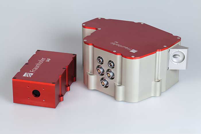
Figure 2. Two 2.X-µm VECSEL laser modules. At (left) is a high-power module with a CW output power up to 3 W and an integrated pump laser in the laser head. The narrow-linewidth module (right) has a free-running linewidth of just 60 kHz (corresponding to 0.8 fm) at 1-W power level in continuous wave operation. Images courtesy of Fraunhofer Institute for Applied Solid State Physics.
>
The quantum defect, in combination with other loss mechanisms, generates a large amount of waste heat in the active region. Therefore, the maximum output power is thermally limited for both pumping schemes, and elaborate heat management techniques are crucial to enable high output powers.
There are two heat management techniques that are frequently used — the intracavity heatspreader and the thin device method — as well as a combination of the two2. The main heat removal pathways of these methods differ (Figure 3). VECSELs in the GaSb material system have specific requirements, as the high reflectivity mirror on the back side of the chip has to be relatively thick. The thermal conductivity of the used materials is comparatively low, which impairs the main thermal pathway of the thin device approach.
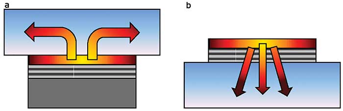
Figure 3. Schematic of the heat extraction pathways for the two most commonly used heat management techniques. The intracavity heatspreader (a, blue) is made from a material with high thermal conductivity, which has to be transparent for pump and laser photons. Then it can be bonded to the front side of the chip and remove the heat directly from the active region (red/yellow) where most of the waste heat originates. The thin-device approach removes heat through the backside of the chip (b), so the thermal resistance of this pathway must be kept as small as possible. Therefore, the backside substrate has to be thinned or completely removed. Images courtesy of Fraunhofer Institute for Applied Solid State Physics.
Therefore, the most commonly used heat extraction method for high-power GaSb-based VECSELs is the intracavity heatspreader. With an intracavity heatspreader made from silicon carbide, output powers up to 7.5 W at 2.0-µm emission wavelength and a heatsink temperature of 20 °C have been realized within a laboratory setting. Heatspreaders made from single crystalline diamond have a much higher thermal conductivity and can increase the output power even further. More than 17 W of output power have been shown in the laboratory, also at 20 °C heatsink temperature and 2.0-µm emission wavelength3.
High-power devices such as these can be used for applications with relative moderate demands for spectral linewidth. For example, they have recently been used to realize a VECSEL-pumped Q-switched Holmium:YAG laser4 with up to 3.3 mJ of output power. Further applications include pumping of Cr:ZnSe or optical parametric oscillators based on zinc germanium phosphide (ZGP) or periodically poled GaAs.
The most common way to achieve single-frequency operation with an intracavity-heatspreader-VECSEL is the introduction of a birefringent filter inside the VECSEL cavity. In addition to the birefringent filter wavelength function, the heatspreader acts as Fabry-Perot etalon due to its parallel surfaces. Therefore, the emission wavelengths of the VECSEL chip are intrinsically limited to the discrete transmission maxima of the heatspreader.
Using a temperature-stabilized resonator, linewidths as low as 60 kHz in free-running operation with up to 1 W of output power can be realized. With active stabilization, 20 kHz is possible. These ultralow linewidths are possible by using an extremely stable housing with low vibrations (Figure 2).
The downside of this setup is that it is very difficult to reach a specific emission wavelength required for a given application. In principle, it is possible to adjust the etalon modes by changing the chip temperature or the pump power. Nevertheless, this method is slow and has severe side effects on other laser characteristics, which limits potential applications.
Thin-device VECSEL at 2.X µm
For precise tuning of the emission wavelength, it is advantageous to omit the intracavity heatspreader and solely use the backside for heat extraction in the thin-device approach. But so far, the output power of GaSb-based VECSELs using this heat extraction scheme has been limited to the few-mW regime5.
A research team at the Fraunhofer Institute for Applied Solid State Physics developed a new process for the fabrication of GaSb-based thin-device VECSELs. With this process, most of the backside substrate can be removed, leaving only a thin layer. While the residual substrate layer can lead to a slight increase in thermal resistance, this method is reliable and delivers
devices with a homogeneous surface quality at a high yield. The chip is soldered to a diamond heatspreader, then soldered to a heatsink made from copper (Figure 4).
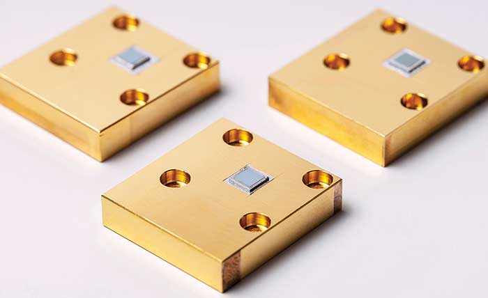
Figure 4. Photo of thin-device VECSEL chips manufactured with the newly developed technological process. The GaSb-based VECSEL chip with a size of 3 × 3 mm is soldered to a diamond heatspreader on top of a gold-plated copper submount. Images courtesy of Fraunhofer Institute for Applied Solid State Physics.
With these thin-device VECSELs, it is possible to reach up to 3 W of output power at 20 °C heatsink temperature and an emission wavelength of 2.0 µm in a high-power, laboratory-scale setup. This is roughly 60 percent of the power that can be achieved with an intracavity heatspreader and the same chip.
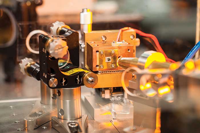
Figure 5. Laboratory setup of a continuously tunable 2.X-µm VECSEL without intracavity heatspreader. Visible is the VECSEL chip with the pump optics on the right, as well as the rotatable etalon and the outcoupling mirror on the left side. With this setup, a single frequency tuning range of 45 nm was shown with an output power over 500 mW. Images courtesy of Fraunhofer Institute for Applied Solid State Physics.
But the real target application of these thin-device VECSELs is not high-power operation, but spectral tunability. In a specifically designed resonator (Figure 5), researchers were able to show single frequency operation with 45-nm continuous (apart from cavity mode hopping) tuning range and up to 500 mW of output power (Figure 6).
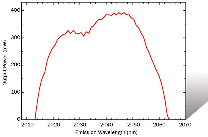
Figure 6. Tuning range of the thin-device laboratory setup. Shown is the output power vs. the emission wavelength. Images courtesy of Fraunhofer Institute for Applied Solid State Physics.
Although the setup was neither optimized for mechanical stability nor temperature stabilized, it showed excellent long-term stability with no mode hop and only 2.2 GHz of temperature-induced wavelength drift over 60 hours of continuous operation.
Overcoming the limitations of the emission wavelength of GaSb-based VECSELs being locked to discrete etalon modes is an important milestone. The thin-device concept enables the use of GaSb-based VECSELs for applications that depend on a light source with a distinct wavelength like quantum optics, laser cooling or the spectroscopy of molecule absorption lines. Additionally, devices without intracavity heatspreaders are well suited as gain material for modelocking, where a broad gain is beneficial.
Meet the authors
Peter Holl holds a degree in physics from the Philipps University of Marburg, Germany, and a Ph.D. from the Fraunhofer Institute for Applied Solid State Physics, Freiburg; email: [email protected].
Marcel Rattunde is head of the department for optoelectronics at Fraunhofer IAF and is working on semiconductor infrared lasers and laser modules; email: [email protected].
References
1. M. Kuznetsov et al. (1997). High-power (>0.5 W CW) diode-pumped vertical-external-cavity surface-emitting semiconductor lasers with circular TEM00 beams. IEEE Photonics Technology Letters, Vol. 9, Issue 8, pp. 1063-1065.
2. P. Holl et al. (2015). Recent advances in power scaling of GaSb-based semiconductor disk lasers. IEEE J Sel Topics Quantum Electron, Vol. 21, Issue 6.
3. P. Holl, M. et al. (2017). GaSb-based VECSEL for high-power applications and Ho-pumping. Proc SPIE, Vol. 10087.
4. K. Scholle et al. (2016). SDL In-band pumped Q-switched 2.1 µm Ho:YAG Laser. Conference on Lasers and Electro-Optics, OSA Technical Digest. Paper STu4M.2.
5. M. Devautour et al. (2013). Thermal management for high-power single-frequency tunable diode-pumped VECSEL emitting in the near- and mid-IR. IEEE J Sel Topics Quantum Electron, Vol. 19, Issue 4.