By applying tunable femtosecond laser pulses, highly desirable all-diamond, large-area coatings with tailored characteristics can be fabricated.
EDUARDO GRANADOS, CERN, AND MIGUEL MARTÍNEZ-CALDERÓN, CEIT
The strongly bound and tightly packed crystal lattice that comprises diamond makes it an ideal candidate for extreme optical and photonic devices. Thanks to the unique combination of its outstanding thermal, mechanical, and optical properties, synthetic diamond is becoming the material of choice for high-power optical and laser systems beyond the kilowatt frontier.
Synthetic diamond’s large index of refraction, normally considered beneficial for optics applications, sets stringent requirements for thin-film antireflection (AR) coatings in order to optimize its transmission at the surface. Unfortunately, combining diamond with inferior materials represents one of its main weaknesses for use in optics and photonics. Multilayer dielectric (MLD) coatings are inferior by about 3 to 4 orders of magnitude (in terms of power handling) to those of the intrinsic diamond, which inevitably leads to increased thermomechanical failures as optical power densities increase to ever higher levels.
However, novel methodologies exist for fabricating all-diamond, large-area coatings with tailored characteristics by using direct femtosecond laser pulses. Laser-induced periodic surface structuring (LIPSS) is a useful technique for fabricating devices capable of spatially manipulating the polarization state of the incident waves, opening the doorway to the fabrication of all-diamond polarizing optics or high-power mode converters.
Fabricated moth-eye coatings
One well-known method for fabricating coatings without using multiple materials is the moth-eye effect1. Here, a material surface is microscopically textured in a pattern with physical features whose dimensions fall well below that of the operational wavelength (Figure 1). The idea is to produce a gradient in the effective optical index of refraction by purely geometrical means. Examples are common in nature and ubiquitous around us. For instance, the outer surface of the cornea of a moth consists of periodic arrays of conical protuberances — termed corneal nipples — with height and spacing below 250 nm. These arrays of subwavelength nipples lead to minimized reflection over a broad range of wavelengths in the visible spectrum and at wide angles of incidence.
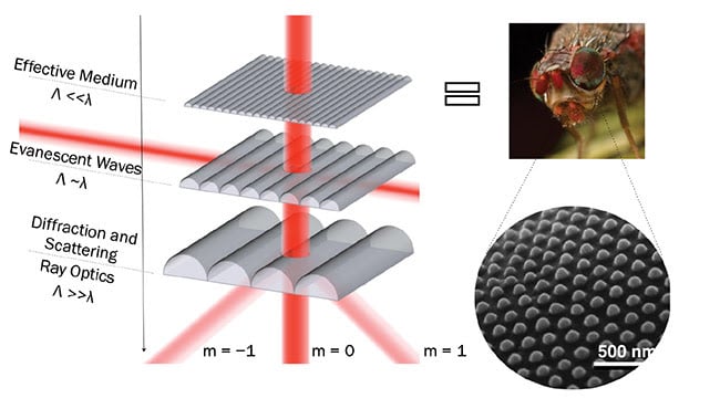
Figure 1. Illustrative scheme of the effective medium moth-eye concept (left). SEM (scanning electron microscope) image a of moth eye, from reference 2 (right). Courtesy of CERN.
The benefit is twofold: A moth, which is inactive during the day, can significantly reduce eye glare and consequently become less visible to predators, while at the same time the moth’s corneal nipples can act as an optically matched layer between the facets of its compound eye and the surrounding air, maximizing the coupling of light into the eye2.
The performance of this moth-eye interface can be predicted based on dielectric mixture models utilizing the optical properties of the base material and surrounding media (air in this case). In the simpler case of periodic surface structures, it can be demonstrated, as shown in the formula below, that the ratio between the structural period (Λ) and the incident light wavelength (λ) needs to be small enough such that only the zeroth diffractive order can propagate into the substrate. Mathematically, this condition can be immediately deduced from the grating equation by forcing the higher diffractive orders to be evanescent:
Here, n1 and n2 are the refractive indices of the surrounding medium and the substrate, respectively; max holds for the maximum of the arguments (n1 and n2); and θ is the incident angle. For example, in order to design a normal incidence diamond moth-eye AR coating operating at a center wavelength of λ ~1 μm, the structure periodicity needs to be Λ < 450 nm. It can also be shown that for each periodicity Λ, the transmission peak is located at different wavelengths, and the transmission bandwidth depends on the morphology and aspect ratio of the surface structures.
In view of the potential advantages of moth-eye coatings, J.F. DeNatale and colleagues demonstrated the first bioinspired diamond AR coating in the early 1990s3. It took almost two decades for the technique to be commercialized, but thanks to developments by companies such as Element Six, it is now common to see all-diamond optics in the mid-IR.
The performance of Element Six’s proprietary material, Diamond PureOptics, is outstanding — an impressive 10× increase in reliability in terms of power density handling when compared to standard MLD AR coating technology. It is not surprising, then, to see microstructured diamond being routinely employed in kW-level CO2 laser systems, with a view toward important application areas such as extreme ultraviolet lithography (EUVL). Extending this capability to other spectral ranges, such as the visible and NIR, is not an easy task, however. Many of the outstanding properties that make diamond interesting, such as damage resistance, chemical inertness, and high thermal conductivity, also make it extraordinarily difficult to process further at the nanoscale.
Machining with nanometer accuracy
The conventional techniques for nanoprocessing other semiconductors, such as silicon, are rather ineffective in diamond and cannot produce the range of structures required for most optics applications. Specialized processing techniques exist for diamond — including reactive-ion etching (RIE), ion implantation with chemical etching, and laser ablation — but they are not always easy or effective. RIE and ion implantation generally require complex chemical processes. And ablation does not enable sufficient resolution for advanced optical applications. For example, state-of-the-art technology for patterning in 2D structures, with a resolution of approximately 100 nm, can be accomplished only with a complex combination of electron-beam lithography and RIE. The lack of a simple or direct fabrication technique that enables the construction of clean 3D nanostructures continues to be a technological barrier that hinders progress.
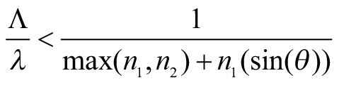
With the relatively recent development of high average power, high repetition rate, and ultrafast fiber lasers, direct laser surface nanofabrication via LIPSS has experienced a renaissance. LIPSS formation was discovered in the 1960s by Milton Birnbaum and colleagues4, shortly after the invention of the laser. More recently, LIPSS was found to be a universal phenomenon that occurs on most solids upon irradiation with ultrafast linearly polarized laser pulses5 (Figure 2a).
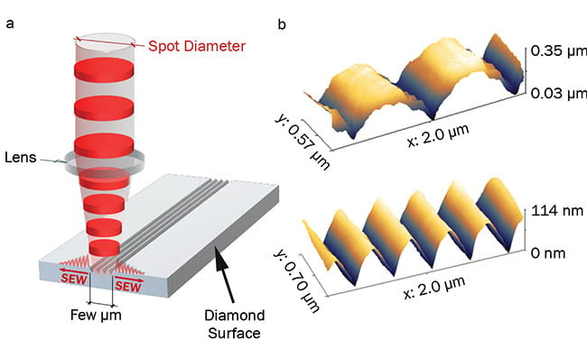
Figure 2. Illustration of the laser-induced periodic surface structuring (LIPSS) fabrication process. Polarization is normally perpendicular to scanning direction (a). Fabricated LIPSS nanopatterns on a diamond surface (b) with two different driving laser wavelengths: λ1 = 800 nm (top); λ2 = 400 nm (bottom). Courtesy of CEIT. SEW: surface electromagnetic waves.
LIPSS consists in a surface relief composed of (quasi-) periodic lines, which mainly depend on both the wavelength and the polarization of the impinging radiation. Typically, LIPSS is generated via spatially modulated material ablation or melting mechanisms, and is assisted by surface plasmon polariton excitation. In this formula, LIPSS patterns usually exhibit spatial periods, or Λ (the distance between the quasi-periodic lines) close to or slightly smaller than the irradiation wavelength, λL, and are called low spatial frequency LIPSS (LSFL): λL/2 ≤ ΛLSFL ≤ λL
For some irradiation conditions, the existence of LIPSS with Λ much smaller than half of the irradiation wavelength (Λ < λL/2) has been demonstrated. These are known as high spatial frequency LIPSS (HSFL), and they tend to be less robust and homogeneous than an LSFL.
LIPSS formation involves multiple mechanisms and a complex sequence of inter- and intrapulse physical processes5. Paradoxically, even though the underlying physical phenomenon of LIPSS is
complicated, they are indeed simple to fabricate. There is still debate about the details, but the models introduced by J.E. Sipe and colleagues6 are generally accepted. LSFL-type LIPSS formation is explained through to the interaction of the incident laser beam with a surface electromagnetic wave (SEW) scattered at the irradiated sample surface, causing a spatially modulated intensity that leads to nanostructure formation (Figure 2b).
The LIPSS orientation is usually (but not always) perpendicular to the laser beam polarization, and the spatial period typically ranges between 0.6λL < Λ < λL. In particular, for semiconductors such as diamond, the period Λ can be approximated with this formula: Λ = λ(η + sin θ).
Here, η = Re [(ε/(ε + 1)]1/2 is the real part of the effective refractive index of the air/diamond interface for surface plasmons,
ε is the dielectric constant, and θ is the incidence angle of the laser light.
Direct control of the period Λ is easily achieved by tuning the laser wavelength and/or the angle of incidence. For optics applications, the aspect ratio of the structures also becomes
relevant, but as it was recently demonstrated, it can also be controlled by carefully tuning the applied fluence and the number of impinging pulses7. In contrast to other materials, with diamond,
the period Λ and aspect ratio can be adjusted quasi-independently, which is particularly advantageous for producing coatings with customized characteristics.
Optimizing transmission
Figure 3. Transmission of LIPSS on diamond substrate with period Λ = 500 nm as a function of LIPSS spatial aspect ratio and incident wavelength λ. Courtesy of CEIT.
A maximum value of transmission (T) ~94 percent for an aspect ratio of 0.4 was experimentally demonstrated (compared to a T ~82 percent for a standard polished diamond surface). This reflectivity reduction can be further optimized by adjusting the LIPSS height, reaching a maximum of nearly 100 percent for an aspect ratio of 0.65 (Figure 3). Controlling the geometry and periodicity of diamond LIPSS nanopatterns can also lead to a strong birefringence, which can be exploited in important applications in high-power waveplate fabrication, currently a subject of intense research. This capability was also tested to fabricate, for example, a vortex beam transformer (or segmented waveplate) fabricated exclusively using LIPSS technology (Figure 4). In this device, the polarization of the impinging wave was modified spatially according to the surface patterns, converting a linearly polarized transverse electromagnetic (TEM00) mode into a transverse magnetic (TM01) radially polarized mode.
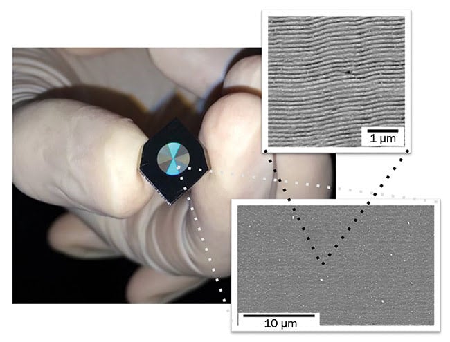
Figure 4. Segmented waveplate fabricated with LIPSS nanopatterns of different orientations in order to convert linearly polarized beams to radially polarized (vortex) beams. Courtesy of Noemi Casquero/CEIT.
Extending the technique to large processed areas is required for optical devices, where spatial coherence or spatial structural phase distribution of the LIPSS nanopatterns becomes crucial8. It has been demonstrated that processing the material surface by scanning the laser beam in successive adjacent passes can generate aligned, regular, and homogeneous structures with nanometer accuracy — but what is the limit? Mysteriously, LIPSS nanopatterns seem to automatically align spatially down to the nanometer scale even when there is no overlap between consecutive passes8. Some theories attribute this behavior to an extension of the plasmonic interaction with nearby LIPSS structures beyond the laser spot size (Figure 5), but this is still unclear.
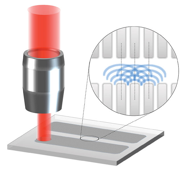
Figure 5. Experimental results indicate that the spatial coherence of the LIPSS patterns is maintained for values of the distance between adjacent passes well beyond the spot radius or the irradiated area. In the offset circle, the blue waves symbolize plasmonic waves. Courtesy of CERN.
Our experimental results indicate that the LIPSS nanostructuring technique can be easily applied to diamond, paving the way to all-diamond metamaterial optics fabrication using exclusively femtosecond laser pulses. LIPSS has already proven to be a mature, scalable, and effective technique for nanomachining virtually any material, with diverse applications covering not only optics but also other surface processes such as enhancement of surface wettability, catalysis, or heat transfer, to name a few.
About the authors
Eduardo Granados has a Ph.D. from Macquarie University and is a staff scientist at CERN researching diamond photonics. Previously, he held appointments at SLAC/Stanford University and MIT. His research interests include light-matter interaction in diamond and ultrafast phenomena; email: eduardo.granados
@cern.ch.
Miguel Martínez-Calderón completed his Ph.D. thesis on ultrafast laser micro/nanofabrication of advanced material surfaces at CEIT-IK4 and the University of Navarra in 2018. He is a junior researcher at CEIT-IK4 and focuses on advancements in ultrafast laser science; email: [email protected].
References
1. P.B. Clapham and M.C. Hutley (1973). Reduction of lens reflexion by the “moth eye” principle. Nature, Vol. 244, p. 281, https://doi.org/10.1038/244281a0.
2. D.G. Stavenga et al. (2006). Light on the moth-eye corneal nipple array of butterflies. Proc R Soc B Biol Sci, Vol. 273, pp. 661-667, https://doi.org/10.1098/rspb.2005.3369.
3. J.F. DeNatale et al. (1992). Fabrication and characterization of diamond moth eye antireflective surfaces on Ge. J Appl Phys, Vol. 71, pp. 1388-1393, https://doi.org/10.1063/1.351259.
4. M. Birnbaum (1965). Semiconductor surface damage produced by ruby lasers. J Appl Phys, Vol. 36, pp. 3688-3689, https://doi.org/10.1063/1.1703071.
5. J. Bonse et al. (2017). Laser-induced periodic surface structures — a scientific evergreen. IEEE J Sel Top Quantum Electron, Vol. 23, p. 1, https://doi.org/10.1109/JSTQE.2016.2614183.
6. J.E. Sipe et al. (1983). Laser-induced periodic surface structure. I. Theory. Phys Rev B, Vol. 27, pp. 1141-1154, https://doi.org/10.1103/PhysRevB.27.1141.
7. M. Martínez-Calderón et al. (2018). Tailoring diamond’s optical properties via direct femtosecond laser nanostructuring. Sci Rep, Vol. 8, pp. 1-9, https://doi.org/10.1038/s41598-018-32520-0.
8. I. Gnilitskyi et al. (2017). High-speed manufacturing of highly regular femto-second laser-induced periodic surface structures: physical origin of regularity. Sci Rep, Vol. 7, p. 8485, https://doi.org/10.1038/s41598-017-08788-z.