The Quantum Flex Platform will become the first accessible 300-mm platform developed for quantum systems.
LEAH SCOTT, LEWIS G. CARPENTER, AND GERALD LEAKE, AIM PHOTONICS
Considerable advancements during the last decade have begun to reveal the critical role of integrated photonics for the successful construction and scaling of quantum systems. Broadly, these industry- and R&D-led efforts are defining the possibilities of this technological space. As support for future quantum technologies continues to grow, so does the anticipation that advancements in this area will soon transition into commercial realities.
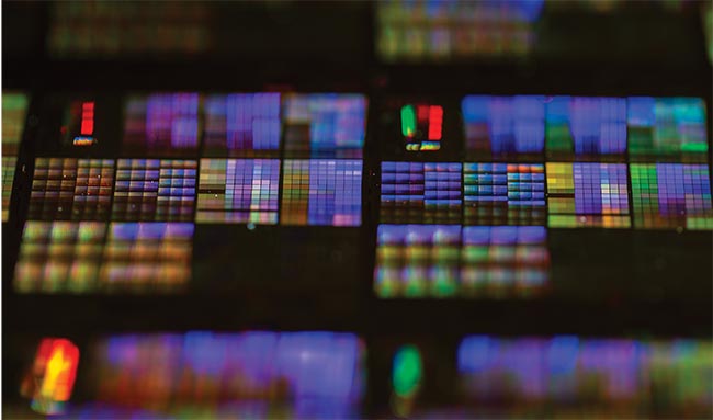
Two reticles of arrays of photonic crystal cavities. Courtesy of AIM Photonics and the Air Force Research Lab (AFRL/Rome, N.Y.).
At the same time, widely accessible capabilities that can be easily leveraged by the quantum community have yet to be realized. Growth of the industrial base today relies on the emergence of an openly accessible photonic integrated circuit (PIC) foundry process capable of meeting the challenging requirements associated with quantum systems.
Inherently, such a solution must enable qubits to be implemented across various frequencies, from the ultraviolet (UV) to the telecommunications (infrared) regimes.
The Quantum Flex Platform (QFlex) developed at the American Institute of Manufacturing Integrated Photonics (AIM Photonics) is addressing this need and working to provide early access to quantum photonics capabilities for U.S. organizations. QFlex is focused on producing an application-specific PIC offering for quantum technologies. At present, it is
positioned to be the first accessible
300-mm platform developed to address the distinct needs of quantum systems.
At the heart of QFlex
QFlex offers low-loss silicon and silicon nitride waveguides with propagation losses as low as 0.1 dB/cm. At the same time, the platform still provides access to active optoelectronic devices such as photodiodes and Mach-Zehnder and ring modulators, all based on doped silicon and/or germanium. QFlex can support both active and passive optical devices, including lasers, low-loss fiber attachments, thermal isolation trenches, and various additional trenches for the post-process integration of heterogeneous materials. The platform supports data communications and telecommunications bands and offers active devices such as PIN photodiodes and ring and Mach-Zehnder modulators that have 3-dB bandwidths exceeding 30 GHz.
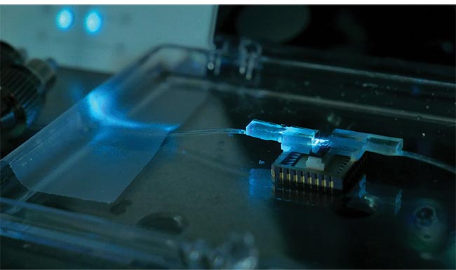
An openly accessible photonic integrated circuit (PIC) foundry process targeting quantum system requirements must enable qubits to be implemented across various frequencies, from the UV to the infrared. This packaged quantum photonic system features low-loss visible optical and electrical input/output. Courtesy of AIM Photonics.
The first release of the QFlex process design kit (PDK) is earmarked for later this year. This PDK will feature components and associated models identifying radio frequency and optical performance with statistically verified compact models. PDK offerings with augmented component libraries are scheduled to be released during the next five years and will be available through commercial and open layout formats.
These offerings are designed to include documentation with measured data and process stack files for custom component development. This is essential for quantum-enabled systems to address practical, real-world needs and applications. AIM Photonics is also working to accelerate the quantum photonics community’s adoption of PICs by providing access to the platform through a recent design
competition, QFlexDC, an initiative that will provide as many as 20 organizations with complimentary QFlex PICs.
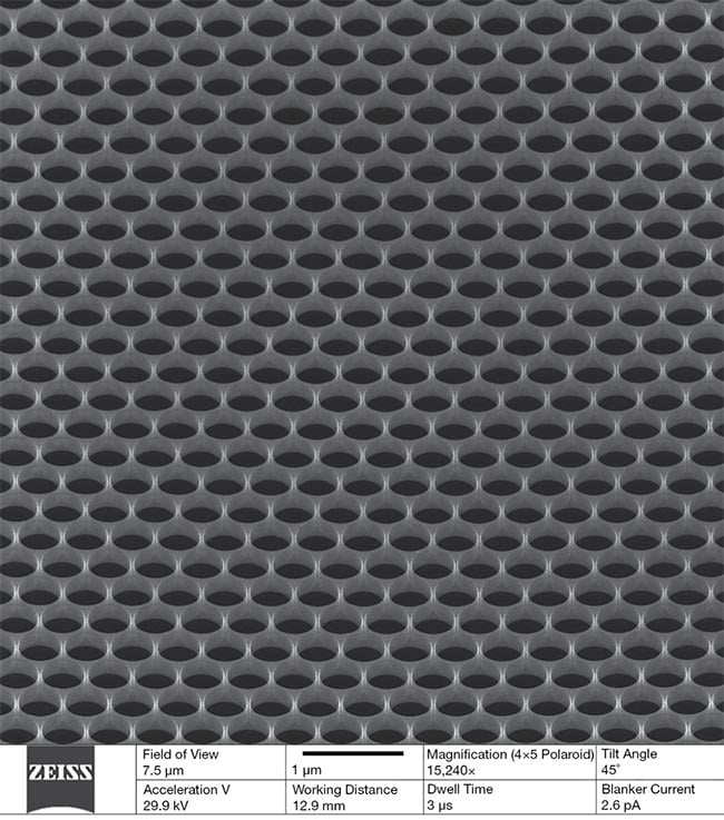
A close-up view of a silicon photonic crystal with quality factors of 10 million. Courtesy of AIM Photonics and the Air Force Research Lab (AFRL/Rome, N.Y.).
By releasing QFlex as a new multiple-project wafer offering as part of its suite of offerings, AIM Photonics can begin to work with members of the U.S.-based quantum community to support their
current needs. The release will also
facilitate continued growth of the platform into a transformative capability to
help develop quantum applications to technology readiness level (TRL) ~7.
Supported application areas include quantum computing, networking, timing, and sensing.
Quantum dynamics
Previously, AIM Photonics collaborated with government partners to develop high-performance quantum capabilities, and subsequent platforms, enabling
excellent performance in the visible and UV regions. PIC platforms to date, however, have focused heavily on operating wavelengths in the O, S, C, and L bands
(1260 to 1360 nm and 1480 to 1610 nm, respectively). This is due to their applicability in data communications and
telecommunications applications. Quantum applications require working with wavelengths in the visible and UV in addition to the O, S, C, and L bands.
Realizing UV to telecommunications operation on a PIC and its optoelectronic control serves to increase the number of different types of qubits that can interface with a PIC. Barium ions, for example, which are studied particularly for quantum capabilities, could be trapped on a QFlex PIC with the expanded wavelength range, since the photonic control beams are in the red (650 nm) and blue (494 nm) with megahertz radio frequency trapping fields. PICs trapping barium are used for a range of quantum systems, including computation, memory, and sensing. The low size, weight, and power of the PICs offers the manufacturability and repeatability benefits of 300-mm CMOS fabrication. The expanded window of operation supported by existing platforms that offer strong performance in the
visible and UV regions can be used to unlock PIC-based quantum applications and their miniaturization.
Ongoing efforts
In integrated photonics, most are aware that launching a multiple-project wafer platform is a major feat. It requires significant commitments of time, talent, expertise, and capital to move from the bench into the commercial space. The QFlex platform effort is bolstered by the Department of Defense funding initiated by the Air Force Research Lab (AFRL) in Rome, N.Y., with additional support from the Micro Electronics Commons Northeast Regional Defense Technology Hub’s (NORDTECH) Quantum Ultra-Broadband Photonic Integrated Circuits and Systems (QUPICS), and the Heterogeneous Quantum Networking projects.
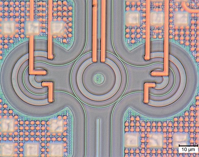
Advancements in single-photon sources have further established this enabling technology for quantum integrated photonics systems. This single-photon source shows silicon waveguides, heaters, and copper wiring. Courtesy of AIM Photonics.
Current work that is aimed at broadening QFlex’s operational spectrum into
the visible and UV stands at TRL 3 and is targeted to reach TRL 6 in 2029. For visible, passive, and active components, as well as nonlinear elements, research efforts are ongoing to add optical materials to the stack. These materials include alumina, aluminum nitride, and thick silicon nitride (~0.8 µm). Upcoming additions to the current QFlex PDK are focused on transmission characteristics in the visible and UV with propagation losses in the decibel per centimeter range, and electro-optic modulation of visible signals in the tens of gigahertz range.
Obtaining early access to these capabilities for U.S.-based organizations
performing R&D in quantum systems will be a critical step toward unlocking the potential of quantum systems and applications.
Meet the authors
Leah Scott is director of communications and information management at AIM Photonics. She has served in leadership roles in higher education and R&D during the last 20 years and has been cited as a contributing author in emerging tech publications; email: [email protected].
Lewis G. Carpenter is the photonics development manager at AIM Photonics. He has 16 years of research experience focused on integrated photonics R&D and on industrially relevant technologies to grow PIC adoption in quantum and sensing; email: [email protected].
Gerald Leake specializes in advanced CMOS, silicon and quantum photonics, and III-V heteroepitaxy lasers for silicon photonics. Part of AIM Photonics’ senior engineering team, he has more than 25 years of experience
in advanced semiconductor tech; email: [email protected].