AR surfaces with subwavelength surface-relief features provide ultrabroadband and angle-insensitive performance with the potential for higher laser-damage thresholds compared to thin-film coatings.
SHELBY AMENT, EDMUND OPTICS INC.
Antireflection (AR) coatings are essential for applications where light throughput is critical, or where backreflections cause issues. Such issues range from ghosts and glare in imaging
applications to unwanted feedback or stray beams in laser applications. For a typical glass substrate, 4% to 8% of visible light is reflected off each bare surface, which can add up in multielement optical systems.
Colorized subwavelength antirelection surfaces. Courtesy of Edmund Optics.
Traditional thin-film AR coatings consist of multiple layers of materials deposited on a surface. These layers have distinct thicknesses and refractive index values tuned to achieve destructive interference at a specific wavelength or range of wavelengths. By design, such stacks are sensitive to both wavelength and angle of incidence, limiting their operating range. Additionally, these coatings can have a number of failure modes in harsh environments and high-laser-power applications such as radiation damage and delamination, often at the interfaces between different materials1.
An alternative approach to traditional AR coatings is the so-called moth-eye effect, which was discovered in the 1960s by C.G. Bernhard and W.H. Miller2. The moth’s eye consists of a hexagonal array of bumps with spacing between them of less than a wavelength of visible light. Such structures present themselves as a continuous refractive index from the immersion material into the substrate material. It turns out that by creating a subwavelength surface relief, an AR
effect can be achieved over a much broader wavelength and angular range than is possible with a thin-film approach (Figure 1).
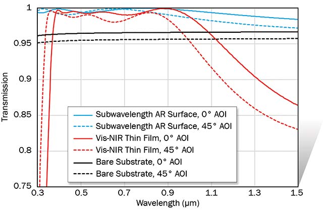
Figure 1. Simulation demonstrating the broad wavelength and angle of incidence (AOI) operation of a
subwavelength AR surface on a fused silica substrate, compared to a thin-film-coated surface.
The subwavelength surface maintains transmission greater than the substrate transmission over a
300- to 1500-nm wavelength range and 0° to 45° AOI range. Note: The vertical axis transmission scale is set to 0.75 to 1 to enhance details. Courtesy of Edmund Optics.
Additionally, an increasing body of evidence shows subwavelength AR surfaces can achieve a higher laser-damage threshold compared to thin-film coatings3. Interestingly, laser damage in structured surfaces often manifests as a melting of the structures themselves, leading to higher Fresnel reflection but otherwise doing no damage to the optic4.
Because of the broadband and wide
angular operation of subwavelength AR surfaces, as well as their damage threshold possibilities, these surfaces are gaining traction in applications as wide ranging as treating solar cell surfaces, reducing glint in military applications, increasing throughput in fibers, and reducing stray light in high-power medical and materials processing laser systems.
Subwavelength surfaces
Methods to model the optical performance of a subwavelength AR surface5 include the effective-medium theory (EMT) and rigorous coupled-wave analysis (RCWA).
In EMT, an effective refractive index for the subwavelength structure is
determined by taking horizontal slices through a cross section of the structure and determining the volume ratio of the substrate material to immersion material.
The resulting fill factor is used to calculate an effective refractive index for
each slice of the structure. In this way,
the structure can be built up and modeled using typical thin-film analysis (Figure 2).
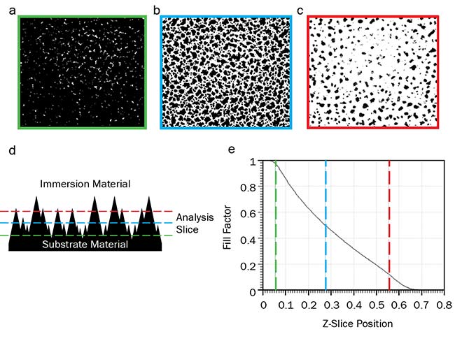
Figure 2. In EMT, an effective refractive index is calculated by analyzing the fill factor for discrete analysis slices. Top-down views of the surface at three different depths of the surface indicating the amount of substrate material (black) and immersion material (white) for the slice (a, b, c). A cross section of the
subwavelength AR surface (d). A plot of fill factor (the ratio of substrate material to immersion material) versus Z slice (e). Courtesy of Edmund Optics.
EMT is limited in its accuracy. Most importantly, it will not capture diffraction and scattering effects present for wavelengths on the order of (and smaller than) the size of the surface features. The method does, however, provide helpful insights for understanding the performance of a subwavelength surface. One takeaway is that reflectance is minimized when the effective medium smoothly transitions from substrate into air, which means a structure with vertical sidewalls such as cylindrical protuberances will not have optimal antireflective properties.
There are several possible types of smoothly varying effective index profiles. Researchers have compared linear, cubic, and quintic profiles and found that the quintic profile produces the lowest reflectance6. This result can be used to inform which cross-sectional shape is most beneficial for the subwavelength surface texture.
To account for diffraction effects, the subwavelength surface should be modeled with a more rigorous approach. One such model is RCWA, which is a solution to Maxwell’s equations in the special case of periodic structures. This model assumes a unit cell that repeats infinitely in the X and Y directions. Within the unit cell, a refractive index distribution or surface-relief structure is defined. Because distinct lateral features are modeled, RCWA is able to capture the loss of spectral transmission as wavelengths approach the feature size of the structure and get distributed into various diffraction orders.
Maximizing broadband operation
The two limits to the antireflection operation of a subwavelength surface are diffraction and transition depth. To understand these limits, RCWA of a rectangular pyramid surface relief in fused silica glass can be examined.
On the short wavelength end, wavelengths approaching the feature size of the structure will begin to diffract. A good rule of thumb is to select a feature period that is less than 0.7× the shortest operating wavelength. When pyramid gratings are compared with different
periods and a 1-1, period-to-height ratio
is applied, it becomes apparent that as
the feature size increases, more light is sent into transmitted and reflected diffraction orders. This diffraction falloff shifts to longer wavelengths as pyramid size increases (Figure 3).
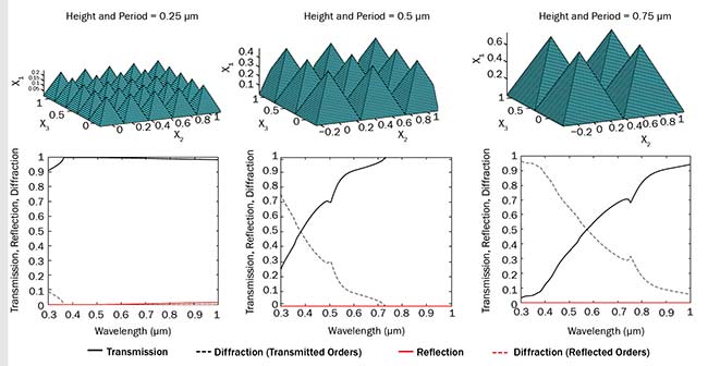
Figure 3. This RCWA simulation of three rectangular pyramid gratings at normal incidence shows the impact of feature size on diffraction (top). Corresponding plots show distribution of light into specular transmission, specular reflection, and diffraction components (bottom). Courtesy of Edmund Optics.
In the long wavelength limit, the height of the subwavelength features is important. As a rule of thumb, the feature height should be greater than 0.4× the longest operating wavelength. This will ensure a gradual transition of refractive
index, allowing light to effectively
transfer into the material7. The impact
of feature height is shown in Figure 4, where structures with 0.1, 0.2, and 0.4 µm in height are compared. The antireflective property falls off beyond 0.25-, 0.5-, and 1-µm wavelengths, respectively.
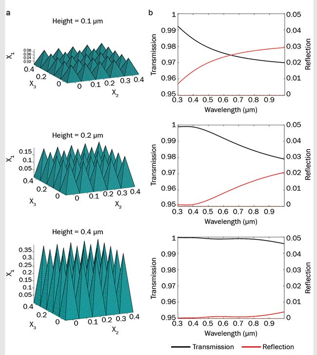
Figure 4. RCWA simulation of three rectangular pyramid gratings at normal incidence shows impact of feature height on transmission. All three surfaces have a period of 0.1 µm (a). Corresponding plots of transmission and reflectance versus wavelength (b). Note: The scale of the transmission ranges from 0.95 to 1, and the scale of the reflectance ranges from 0 to 0.05. Courtesy of Edmund Optics.
Fabrication
Researchers have experimented with subwavelength surface texturing to reduce reflection since the 1970s, shortly after discovering the moth-eye effect8. Approaches to fabricating structured
AR surfaces include photolithography,
e-beam lithography, self-assembly,
embossing, solution processing, glancing-
angle physical vapor deposition, and
wet/dry etching9. Some methods result
in periodic structures, while others result in a random structure of a general feature size. An important aspect to consider in selecting fabrication technique is the time, cost, and scalability of manufacturing. One method with the potential to scale up for manufacturability is a dry etching process using a random metallic nanoisland mask10.
Metallic nanoisland formation has
been used by researchers for enhancing
signals in surface-enhanced Raman
spectroscopy, ultrasensitive detectors,
and biosensors. In this case, nanoislands serve as a mask for a dry etching process. By controlling process parameters, the size and spacing of the nanoislands can
be adjusted (Figure 5).
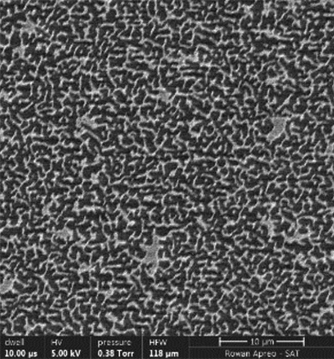
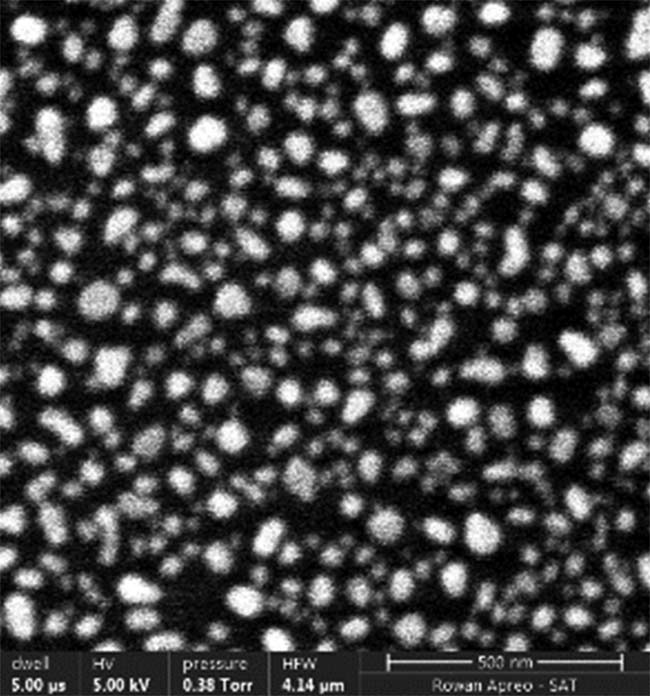
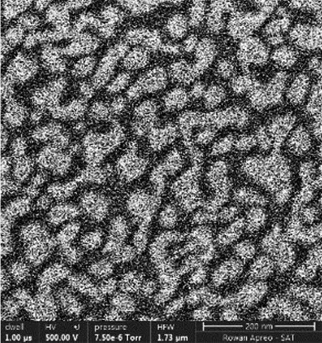
Figure 5. While the exact size and spacing of the nanoislands are random, as shown in these scanning electron microscopy (SEM) images, each mask has a general feature size that is tuned for the desired operating wavelength range. Feature size ˜1.5 µm (top). Feature size ˜100 nm(center). Feature size ˜60 nm (bottom). Courtesy of Edmund Optics.
With the nanoisland masks in place, the glass is etched using an inductively coupled plasma reactive-ion-etching
(ICP-RIE) system. In this system, an oscillating current in a coil creates a
magnetic field that strips molecules in a gas mixture of their electrons, creating
a plasma. In addition, the lower platen that holds the parts is capacitively coupled to a second radio-frequency (RF) power supply. This creates an electric field that draws positively charged ions in the plasma toward the sample.
In the ICP-RIE system, there are two etching mechanisms. Heavy argon ions bombard the surface and sputter away
the mask and the glass alike, while
reactive ions chemically react with the glass and carry it away. By controlling process parameters such as gas mixture, plasma density, vacuum pressure, and
ICP and RF powers, unmasked regions
of the glass can be etched to a specific depth while the width of the nanoislands is simultaneously reduced. The goal
of this process is to achieve a tapered
structure with a shape and height distribution that produces ideal AR characteristics.
A variety of subwavelength structures has been fabricated using this technique, several of which exhibit broadband AR properties (Figure 6).
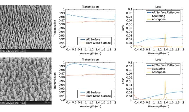
Figure 6. Two examples of subwavelength AR structures in fused silica. SEM images give a sense of the scale and shape of the features (left). Transmission plots, measured using a Lambda 1050 spectrophotometer, comparing single-surface transmission of the subwavelength AR surface to a planar surface at normal incidence. Note: The scale of the transmission ranges from 0.9 to 1 (center). Various loss mechanisms are also measured. Absorption of the glass is noted for reference. Note: The scale of the absorption and reflection ranges from 0 to 0.1 (right). Courtesy of Edmund Optics.
Subwavelength surface texturing is a method used to achieve AR properties
on a surface over a wide range of wavelengths and incidence angles. Unlike thin-film coatings, which operate based on interference of light between layers, surface texturing acts as a refractive index gradient. Subwavelength surface texturing is a fascinating technique that shows great theoretical potential for achieving ultrabroadband and angle-insensitive AR properties. In addition, the structured
surfaces lack the adhesion and local heating concerns that affect durability and laser damage in thin-film AR coatings.
Meet the author
Shelby Ament is an optical research engineer for Edmund Optics Inc.; email: [email protected].
References
1. R.J. Weiblen et al. (2015). Irradiance enhancement and increased laser damage threshold in As 2 S 3 moth-eye antireflective structures. Opt Lett, Vol. 40, Issue 20, pp. 4799-4802.
2. C.G. Bernhard (1967). Structural and functional adaptation in a visual system. Endeavour, Vol. 26, Issue 98, pp. 79-84.
3. L.E. Busse et al. (2015). Review of antireflective surface structures on laser optics and windows. Appl Opt, Vol. 54, Issue 31, pp. F303-F310.
4. L.E. Busse et al. (2014). Anti-reflective surface structures for spinel ceramics and fused silica windows, lenses and optical fibers. Opt Mater Express, Vol. 4, Issue 12, pp. 2504-2515.
5. K. Han and C.H. Chang (2014). Numerical modeling of sub-wavelength anti-reflective structures for solar module applications. Nanomaterials, Vol. 4, Issue 1, pp. 87-128.
6. J.-Q. Xi et al. (2007). Optical thin-film materials with low refractive index for broadband elimination of Fresnel reflection. Nat Photonics, Vol. 1, Issue 3, pp. 176-179.
7. T. Lohmueller et al. (2010). Improved properties of optical surfaces by following the example of the “moth eye.” In Biomimetics: Learning from Nature. Amitava Mukherjee, ed. London: IntechOpen Ltd.
8. M.J. Minot (1976). Single-layer, gradient refractive index antireflection films effective from 0.35 to 2.5 µ. JOSA, Vol. 66, Issue 6, pp. 515-519.
9. S. Chattopadhyay et al. (2010). Anti-reflecting and photonic nanostructures. Mater Sc Eng R Rep, Vol. 69, Issue 1,pp. 1-35.
10. D. Infante (2013). Durable, superhydrophobic, antireflection, and low haze glass surfaces using scalable metal dewetting nanostructuring. Nano Res, Vol. 6, Issue 6, pp. 429-440.