Amid EUV rollout delays and the spread of 5G and AI, pressure is growing on DUV laser suppliers to lower costs and boost throughput.
JAMES SCHLETT, CONTRIBUTING EDITOR
Four years ago, several leading-edge chip foundries raced to roll out extreme-ultraviolet (EUV) lithography processes for sub-14-nm chips that were intended to succeed the preceding generation of chips. Then, in the summer of 2018, GLOBALFOUNDRIES announced that it was abruptly halting its plans for 7-nm chip development to focus instead on a 14-nm lithography process and a 12-nm leading performance (12LP) platform that used deep-ultraviolet (DUV) lithography. The change came as the company saw financial concerns with the transition to the 7-nm EUV lithography node, as well as greater opportunities for DUV processes. The pivot caught the semiconductor device manufacturing industry by surprise, and it indicated a greater trend that is now seeing the DUV process catch a second wind, driving advancements in the lasers that power the systems.
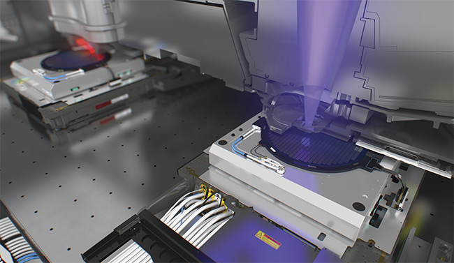
A rendering of one of ASML’s EUV lithography systems during wafer-stage exposure. Next-generation EUV systems can achieve 15× smaller wavelengths than their DUV predecessors by leveraging CO2 laser-produced plasma light sources. Courtesy of ASML
The shift means that complex multipatterning DUV immersion exposures with 193-nm argon fluoride (ArF) lasers are in strong demand — stronger than even their manufacturers expected. These DUV systems increase numerical aperture and resolution by placing a thin film of water between the wafer and the lens. EUV systems, in contrast, can achieve 15× smaller wavelengths (13.5 nm), leveraging CO2 laser-produced plasma light sources that support single-patterning rather than multipatterning exposures. But technical challenges when applying EUV sources have inhibited more widespread industry adoption.
Applications for chips fabricated with DUV immersion systems include 5G, artificial intelligence (AI), and data centers. Such chips are handling ever-rising amounts of data produced by a more connected world via the Internet of Things, as well as increasingly intelligent product platforms, such as automotive systems. These data-generating applications are typically powered by chips made with dry lithography systems fabricated with 248-nm krypton fluoride (KrF) lasers, according to Peter Mayer, an EUV source system architect at ASML San Diego.
Lithography machine manufacturers, such as ASML, expect that the proliferation of advancements in applications, data, and algorithms will continue to drive the need for EUV lithography systems. However, DUV processes will be just as important during the transition because the demand for DUV’s capabilities will extend beyond the EUV tipping point.
Improvements to DUV light sources support rather than detract from the wider adoption of EUV systems. ASML’s EUV roadmap calls for innovations in DUV, metrology, and inspection to supplement the power of EUV-led geometric scaling
or shrinking. Even when GLOBALFOUNDRIES was pursuing 7-nm nodes, it still planned to use both EUV and DUV systems. “The two technologies coexist together and always will,” Mayer said.
EUV crossed the cost-benefit analysis threshold for logic chipmakers in 2019, and leading-edge memory manufacturers are starting to cross that point. They are using EUV on 7- and 5-nm logic nodes and 10-nm-class dynamic random-access memory (DRAM), according to Mayer.
In a February call with investors, however, ASML President and CEO Peter Wennink said demand for the company’s DUV machines has been stronger than the company anticipated. “We have increased our investment in R&D to provide our customers with evermore powerful and productive litho machines to help them deal with the increasing demand and lower cost-per-chip challenges.”
ASML competitor Nikon likewise reported in February that it expects demand for its core ArF immersion lithography systems to remain solid moving forward. This statement came after Nikon’s main customer, Intel, delayed the rollout of its 7-nm chip until 2023.
DUV advantages
In summer 2019, a year after GLOBALFOUNDRIES announced its shift away from EUV, the company demonstrated that its existing DUV processes could deliver significant improvements to its original 12LP platform. Specifically, the company’s new 12LP+ platform for cloud and AI applications could improve chip performance by 20% or reduce power requirements by 40%, as well as improve logic area scaling by 15%.
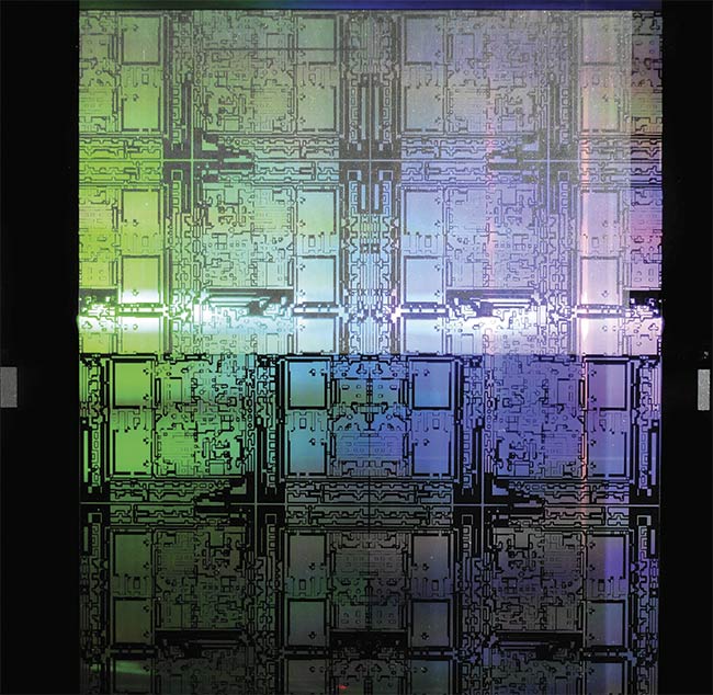
The surging demand for DUV lithography systems is, in turn, putting pressure on the manufacturers of laser writers to increase the throughput of photomasks, which are required for heavy multipatterning DUV lithography processes. Courtesy of Applied Materials.
GLOBALFOUNDRIES’ 12LP and 12LP+ platforms use the same lithography tooling, according to Owen hu, director of integration engineering at the company’s Fab 8 facility in Malta, N.Y. And the 12LP+ power and performance improvements were achieved without changing laser functions or parameters. However, several ArF laser features influenced GLOBALFOUNDRIES’ decision that market opportunities for its DUV lithography systems were better than those for its EUV platforms. These features included advancements in critical dimension uniformity, better overlay control, lower sensitivity to incoming wafer topography, higher reliability with less tool maintenance, and higher throughput.
“DUV will be still needed for noncritical litho layers, even at smaller geometries,” hu said. “EUV serves for the technology-scaling purpose for chip performance and power. However, the high cost of ownership creates a significant cost barrier for the semiconductor industry to migrate to 7 nm and beyond [on] a large scale. Lower-cost DUV, with high throughput to compensate for the high cost of EUV, will help the industry to further improve chip performance and power.”
ArF laser advancements
The improvement of this lower-cost consideration is a major focus of laser innovation at Cymer, a DUV light source supplier and subsidiary of ASML.
“Demand has skyrocketed and we are working not only to produce and deliver DUV systems with new features, but also to make our installed base systems more productive through technology advancements,” said Marshall Benham, Cymer’s managing director of product and service marketing.
One of these new features emerged last summer with Cymer’s seventh-generation ArF light source, the XLR 960ix, which is qualified for ASML’s NXT:2050i immersion system that first shipped in 2020. The laser features new hardware advancements that improve process control, as well as increased availability, sustainability, and productivity for leading-edge
ArF immersion lithography systems.
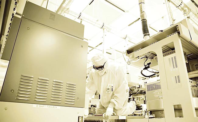
A cleanroom in GLOBALFOUNDRIES’ Fab 8 facility in Malta, N.Y., where the company is using DUV lithography to achieve significant improvements in performance and power requirements for its 14- and 12-nm leading performance platform. Courtesy of GLOBALFOUNDRIES.
“One challenge that cutting-edge
lithography systems face is associated with the intrinsic coherence of a laser source,” Benham said. “In propagating through the optical train of the scanner, self-interference of the laser generates speckle in the image at the wafer. This nonuniformity in intensity causes variation in the exposure of the resist, which leads to critical dimension variation. The XLR 960ix incorporates new optical modules that reduce the speckle contrast by 30%, contributing to reduced linewidth roughness and improved wafer yield.”
On the cost-reduction front, much focus is on extending the laser’s consumable modules, such as the optics and discharge chamber. “Progress on this front has demanded deepening our understanding of the wear mechanisms for these modules, as well as developing new metrology and test capabilities,” Benham said. For example, Cymer’s fifth-generation chamber module is allowing high-volume fabs to run approximately one year between scheduled maintenance.
DUV laser writers
The surging demand for DUV lithography systems is also putting pressure on the manufacturers of laser writers to increase the throughput of photomasks. This poses a different set of challenges for the DUV lasers used to mass-produce the masks, which are required for heavy multipatterning DUV lithography processes.
One recently introduced solution was the Alta 4700DP laser writer from
Applied Materials, which patterns masks 10% to 50% faster than earlier models, using a 257-nm continuous-wave laser rather than a pulsed ArF excimer laser.
The faster patterning is achieved through a new software-based data path that greatly reduces data-handling overhead time. It maximizes the percentage of time the continuous-wave laser is actually printing patterns on the mask, enabling the platform to reach its highest possible throughput, according to Tom Newman, Applied Materials’ senior product marketing manager.
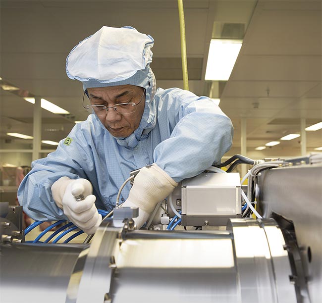
An engineer assembles an illumination module for a DUV lithography system. Improvements to DUV light sources are supporting rather than detracting from the wider adoption of EUV lithography systems. Courtesy of ASML.
“Further increasing the output power of the laser would not increase the throughput because the scanning rate is fixed, and the laser power is attenuated to match the sensitivity of the photoresist on the mask,” Newman said. “However, there are significant benefits from improved laser technology, including a higher quality output beam shape, more stable beam pointing, and reduction in power consumption.”
CO2 laser advancements
One of the biggest laser-related challenges to the wider adoption of EUV is the associated energy consumption. ASML is aiming to reduce the amount of energy its NXE lithography system consumes by more than twofold between 2020 and 2024 via better conversion efficiency, higher productivity, and improved infrastructure. To this end, the company improved the conversion efficiency in the plasma vessel where the CO2 laser wavelength is converted into EUV light. “This is a key sustainability step, as we are able to get more EUV power out [with] the same laser power in,” Mayer said.
“Society’s hunger for chips remains unstilled, driving ever-increasing demand for our EUV and DUV systems, as well as metrology tools and software solutions,” he said. He pointed to International Data Corp.’s forecast that 175 ZB of data will be created per year by 2025. “This is driven by ubiquitous computing, such as multiple machines [communicating with] multiple machines, mobile, automotive, high-performance computing, and the Internet of Things.” It is a cycle, Mayer said, that is driven by enabling Moore’s law through ever-improved lithography performance at lower costs.