New demand for PICs promises to erupt across multiple end markets over the next few years, forcing fabricators to contemplate options for streamlining the optical alignment of these components.
MICHAEL EISENSTEIN, SCIENCE WRITER
The early 2000s saw the rapidly growing global appetite for data collide with the limitations of copper-based wire networks. The performance of these conventional data transmission systems declined dramatically at data bandwidths beyond 10 Gbit/s, imposing a major speed limit on the growth of the internet.
Fortunately, an alternative technology, in which silicon-based photonic devices are coupled to fiber optic cables, was already proving its mettle as a potential replacement. At the time, the technology largely found use along the network backbone. Intel’s CEO, Pat Gelsinger, could see the writing on the wall as early as 2005, when he was a senior vice president at the company. “Today, optics is a niche technology,” he told MIT Technology Review. “Tomorrow, it’s the mainstream of every chip that we build.”
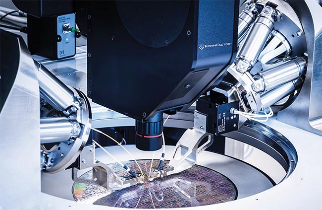
Active alignment systems have
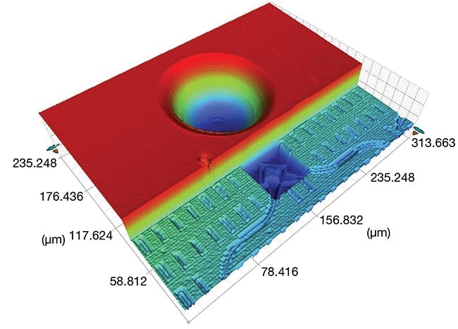
increasingly accelerated the alignment of photonic integrated circuits (PICs) and fiber arrays. PI’s (Physik Instrumente’s) fast multichannel photonics alignment technology, for example, uses sophisticated parallel-processing scanning and optimization algorithms to simultaneously couple multiple arrayed fibers to a silicon photonic chip. The technology configures connections that once took 2 min in roughly 300 ms. Courtesy of Physik Instrumente.
Gelsinger’s statement was prescient. By 2016, Intel was producing its first generation of optical transceivers for use in data centers, where the technology proved capable of relaying data rates of 100 Gbit/s. And today, silicon photonics is widely used in data processing and transmission
applications, where its data speeds steadily creep toward the terabit scale.
Modern silicon photonic integrated circuit (PIC)-based devices offer many advantages compared to standard electronic integrated circuits. PIC devices can be manufactured using many of the same wafer-and-chip fabrication processes, but they consume less power, produce less heat, and can transmit data at higher speeds, without sacrificing signal strength or quality. And, as Gelsinger anticipated, it is now clear that these advantages will have a transformative impact on a range of emerging technologies.
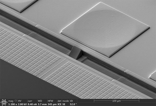
Currently, PICs’ global manufacturing capacity is underprepared for a looming surge in demand. The major limitation is not in manufacturing the chips themselves, but rather in the speed with which the chips can be integrated into electronic devices. Aligning the optical connections is a particular challenge during the packaging process, which, by some estimates, represents 70% of the costs associated with silicon photonic device production. Courtesy of Vanguard Automation.
“Things like chip-based lidar for autonomous driving and safety systems on cars — that’s silicon photonics,” said Scott Jordan, head of photonics at PI (Physik Instrumente). “We’re seeing new biosensors, photonic computing using photons for logic instead of electrons. It’s just been an explosion of new applications.” The still-nascent field of quantum computing will also be a beneficiary of silicon photonics, and Jordan describes PICs as “probably the most consequential development in semiconductors since the integrated circuit.”
But he also sounds a note of caution, warning that today’s manufacturing capacity is underprepared for dealing with the coming surge in demand. “It’s a three-order-of-magnitude jump from what the industry is currently doing right now,” Jordan said.
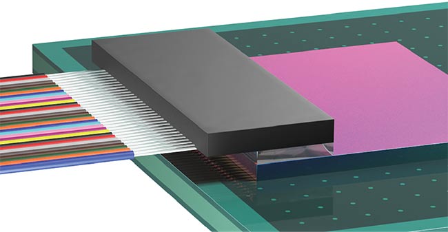
Teramount’s PhotonicPlug technology is designed to facilitate the passive self-alignment of optical components (top). These elements are incorporated during the wafer-level manufacturing process and can increase alignment tolerances to more than ±20 μm/dB to simplify the subsequent alignment of fiber connections. Fibers linked via this technology can also be disconnected and reconnected, allowing alignment to be maintained after performing reflow-based packaging. Courtesy of Teramount.
Teramount’s PhotonicBump components can be incorporated during wafer fabrication to facilitate alignment of fiber connections along the edge of the PIC (bottom). Courtesy of Teramount.
The key challenge is not in manufacturing the photonic chips themselves, but rather in integrating them into electronic devices. Thorsten Mayer, CEO of Vanguard Automation, estimates that 70% of the costs associated with silicon photonic device production arise during this packaging process — in particular, during the laborious process of ensuring that the chips are precisely aligned both with each other and with the optical fibers that relay their photonic signals. The technologies that can facilitate this process are evolving rapidly, but more progress will be needed to keep pace with the rising generation of PIC-based systems.
Making a connection
Forging robust linkages between photonic devices is far more challenging and labor-intensive than it is for conventional electronic integrated circuits. The mode fields — which describe the effective
diameter of a light-emitting surface — must be precisely matched at the point of connection in order to minimize leakage or loss. Even small discrepancies in
optical alignment can lead to severe
degradation of the photonic signal.
Creating a single one-to-one connection was a chore in the early days of the industry. Hesham Taha, co-founder and CEO of Teramount, recalls the state of the field when his company launched in 2015. “We were familiar with aligning fibers to chips with an optical table, micropositioners, etc., and we thought this was only in academia,” he said. “But we found out that industry was not far from there, and it was really challenging to connect a single-mode fiber to silicon photonics chips.”
Automation of active alignment has significantly simplified this process. In this approach, various chips and fibers are assembled into their intended configuration, and light is pumped into the circuit. The alignment system subsequently shifts and fine-tunes the relative positioning of the components, while a sensor monitors the amount of light traveling through the photonic circuit until an ideal positioning with minimal signal loss is achieved.
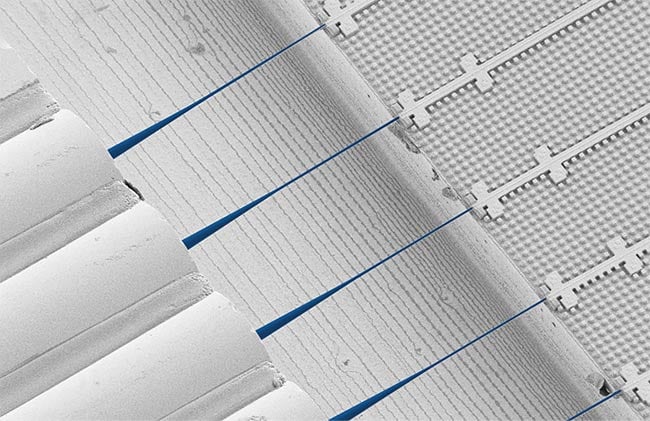
PICs often rely on fiber connections along the chip’s edge. These connections are trickier to align compared to grating couplings that couple the fiber vertically to the top of the chip. PhotonicBump technology aims for a hybrid approach by deflecting beams at edge couplings in a vertical direction to enable wideband surface couplings without fundamentally changing the chip design. Courtesy of Teramount.
Today’s PIC devices are far more complex than first-generation single-mode fiber photonics, and this increases the challenge of alignment exponentially. Individual optical fibers have been replaced by fiber arrays, and a given chip might need to interface with several such arrays simultaneously. “We’re working with some customers that have four or six input arrays, and each array has at least one additional degree of freedom — that is the rotation,” Jordan said. “Every time you make a rotational motion, you do a dealignment of the x- and y-axes.”
As recently as five years ago, this optimization process was prohibitively slow from an industrial manufacturing perspective. “We’re talking in the minutes range,” Mayer said.
Fortunately, modern active alignment systems have become better suited for quickly tackling the fiber array problem. In 2016, for example, Jordan and his colleagues at PI developed an approach called fast multichannel photonics alignment that uses a sophisticated parallel-processing scanning and optimization algorithm to facilitate the simultaneous coupling of multiple arrayed fibers to a silicon photonic chip. “It lets you do all of that in one step,” Jordan said. Connections that would normally take 2 min to configure could now be established in roughly 300 ms. “This system is typically about 100× faster,” he said.
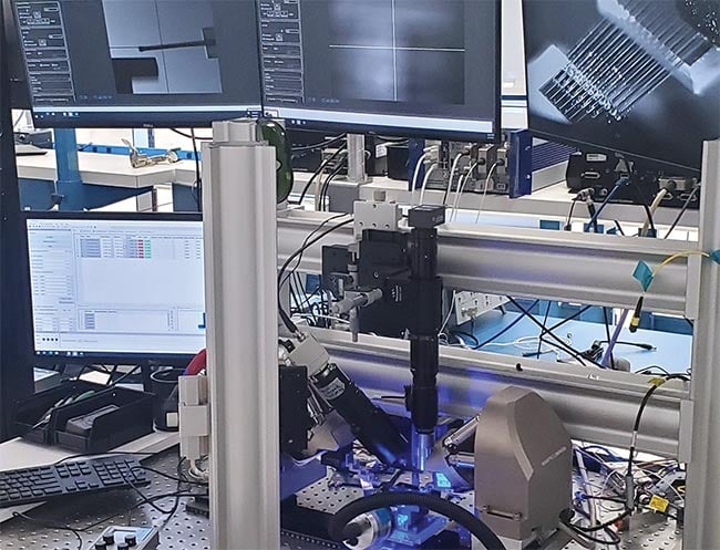
Even with sophisticated automation in play, active alignment is a complex workflow that requires multiple stages of testing and process optimization, said Kevin Pitkin, technology director at contract manufacturing company Benchmark Electronics. Each stage of process development work typically begins with a “dry” alignment of just the optical components themselves, followed by another round of alignment in a refractive index-matched liquid, and then a final application of bonding adhesive.
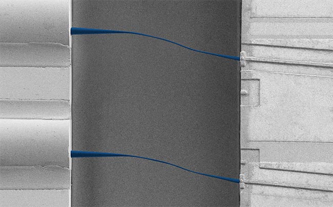
Photonic wire bonding aims for a third alternative to the active or passive alignment of PICs to optical fibers or other components (top). Developed and commercialized by Vanguard Automation on machines built in collaboration with FiconTEC, this approach directly forges the couplings with a ‘3D nanoprinting’-based approach. Courtesy of Vanguard Automation.
Even with the aid of sophisticated automation, actively aligning PIC components and devices requires a complex workflow involving multiple stages of testing and process optimization (bottom). Courtesy of Benchmark Electronics.
“Then the tough part starts,” Pitkin said. And the subsequent curing process can profoundly affect alignment. “It shrinks and pulls, and even a 0.3-µm shift is a big deal when you’re working with a 1-µm waveguide.”
Throughout this process, PIC packagers must continuously test the device to ensure that optimal alignment is being preserved. “You’ve sometimes got to make your decision as to what percent loss you’re going to have going on, and just kind of say, ‘OK, this is what it is,’” he said.
Passive pursuits
Active alignment is the current method
of choice in the PIC industry. Most manufacturers develop their own packaging workflows using alignment instrumentation from companies such as PI. Or they turn to toolmakers such as FiconTEC and Etteplan that develop customized end-to-end fabrication pipelines incorporating such alignment systems.
But other emerging alternatives aim to make alignment less of a resource-intensive process, or even to circumvent it altogether.
“One of the ‘unicorns’ of the photonics industry for 30 years has been passive alignment, where you snap things together like Legos,” Jordan said. “It’s a beautiful dream, but that means that these components sometimes have to be machined with accuracies of 20 nm or so.”
GlobalFoundries offers one such passive alignment system for the photonic chips it manufactures, wherein PICs are fabricated with V-shaped grooves designed to accommodate incoming and outgoing optical fibers that can then be coupled to the chip using a die attach machine. But Pitkin said that routinely achieving effective adhesive bonding without compromising the alignment or stability of the photonic circuit connections in such systems can pose a notable challenge. Nevertheless, GlobalFoundries is making steady progress with this approach and has incorporated its groove-based passive alignment system into the recently launched GF Fotonix PIC manufacturing platform, which is now being tested by major industry partners such as Cisco Systems and NVIDIA.
Teramount is pursuing an alternative approach to passive alignment. “One should relax the tolerances, and not go and address the tight tolerances with more and more precise machines,” Taha said. This is the philosophy underlying the company’s PhotonicPlug — a self-aligning optical component that is incorporated through wafer-level manufacturing processes. The PhotonicPlug can increase tolerances to more than ±20 μm/dB, greatly simplifying the subsequent alignment of fiber connections. A second optical component, PhotonicBump, is also incorporated during wafer fabrication to facilitate alignment of fiber connections at the edge of the PIC. Many photonic chips rely on such connections, which tend to yield lower loss. But these edge connections are also much trickier to align in comparison to grating couplings, where the fiber is coupled vertically to the top of the chip. PhotonicBump achieves the best of both worlds by deflecting beams at edge couplings in a vertical direction, enabling wideband surface coupling without fundamentally changing the chip design.
Taha said incorporating the components at the wafer stage greatly simplifies
the design of co-packaged chips that incorporate sophisticated combinations of electronic and photonic components.
“We have one project we are working on with a partner where we package 64 fibers next to 450 electrical bumps,” he said.
Fibers linked via the PhotonicPlug technology can also be disconnected and reconnected, which means that alignment can be maintained after performing reflow-based packaging — a high-temperature soldering process commonly used in co-packaged electronics. “This
is not doable with active alignment,”
Taha said.
Photonic wire bonding is yet another approach to aligning PICs. Developed and commercialized by Vanguard Automation on machines that were built in collaboration with FiconTEC, this approach directly forges the couplings between fibers, PICs, and other optical components such as lasers and amplifiers by using a precisely targeted laser beam. The connection sites are immersed in a viscous, photosensitive material and analyzed using a sensitive machine vision platform to identify the sites where an interconnect must be established. “Once the machine has detected the interfaces, it calculates on the fly the trajectory and the geometry of the bond,” Mayer said.
A femtosecond laser then establishes the bond along the defined route via
two-photon polymerization. Any remaining photosensitive material is washed away with solvent, and the bonds are coated with a cladding material. The resulting bond exhibits single-mode behavior, he said. “So you avoid any optical loss caused by modal mismatch propagation.”
Mayer estimates that it typically takes ~30 to 60 s to establish these connections, although manufacturers will need to first go through a period of careful process optimization to develop the best bonding strategy for each new PIC device.
Opportunity knocks
For now, active alignment remains the method of choice for the majority of PIC packaging efforts. It is a mature technology with a well-established track record. Alternative contenders such as Teramount and Vanguard Automation are building industry partnerships with the goal of putting their technology in real-world products. But Mayer said this has been a gradual process.
“We’re coming and talking about companies changing their manufacturing technology, which is a mission-critical thing,” he said. “You do not do this overnight.”
Given the high cost associated with building out a packaging workflow, Pitkin said he believes that many contract manufacturers will be reluctant to become early adopters of the new technologies.
Additionally, for manufacturers conducting on-site wafer fabrication, active alignment systems may be a critical component of their larger process. Jordan said that such instruments are often directly coupled to wafer probing systems, which test the quality and performance of each batch of silicon photonic chips prior to the dicing process. “Every wafer has to be tested, because the consequences of packaging bad chips are just so expensive,”
he said. “It’s even more so with photonics because the yields are worse [than with electronic integrated circuits].”
But new investments in technology and packaging capacity will be essential before the silicon photonics era can get fully underway. Right now, Europe and Asia are dominant in this sector, and America is struggling to catch up. “The photonic packaging part of the industry in the United States is almost nonexistent,” Pitkin said. Benchmark Electronics is one of the nation’s few well-established contract manufacturers. “I turn away five customers for every one I take,” he said. And for the time being, contract manufacturers are driving much of the productivity in the PIC sector, although some major industry players — such as Intel — have brought their production processes in-house.
Nevertheless, Jordan is confident that the industry will quickly move past these growing pains. “An ecosystem has emerged, toolmakers have emerged, and today you can build a fab from the ground up just by issuing purchase orders,” he said. “Photonics isn’t there yet, but soon it will be.”