
Atomic Behavior Recorded in Real Time
IBM announced a breakthrough to its 20-year-old scanning tunneling microscope technology on Friday that gives scientists the ability to record, study and visualize the extremely fast spin of electrons inside individual atoms, in real time.
Similar to how a high-speed video camera captures each flap of a hummingbird’s wing, scientists at IBM's Almaden Research Center in San Jose are using the scanning tunneling microscope (STM) like a high-speed camera to record the behavior of individual atoms at a speed about one million times faster than previously possible.
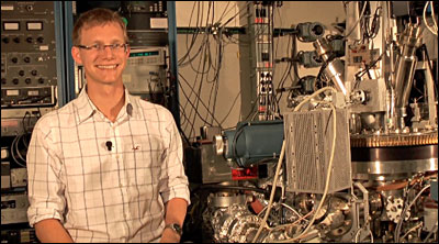
Almaden Post Doctoral Researcher in Nanoscale Studies, Sebastian Loth, next to the nobel-prize winning Scanning Tunneling Microscope. (Images: IBM)
Since the magnetic spin of an atom changes too fast to measure directly using previously available STM techniques, time-dependent behavior is recorded stroboscopically, in a manner similar to the techniques first used in creating motion pictures, or like in time lapse photography today.
"In order to measure the time evolution of magnetic atoms, we had to employ a trick," said Sebastian Loth, Almaden post doctoral researcher. "We had to use a pump-probe technique that takes the movie one frame at a time. that means that we hit the magentic atoms with a bunch of electrons, they excite the magnetic atom and induce the dynamical behavior. Then we just wait a while -- a few nanoseconds usually -- and then we take a snapshot of this atom at that point in time. And then we repeat it -- we hit the atom again with electrons, we wait a little longer now, and take another snapshot. And in this way, we record the movie, frame by frame."
For each time increment, the scientists repeat the alternating voltage pulses about 100,000 times, which takes less than one second.
In the experiment, iron atoms were deposited onto an insulating layer only one atom thick and supported on a copper crystal. This surface was selected to allow the atoms to be probed electrically while retaining their magnetism. The iron atoms were then positioned with atomic precision next to nonmagnetic copper atoms in order to control the interaction of the iron with the local environment of nearby atoms.
The resulting structures were then measured in the presence of different magnetic fields to reveal that the speed at which they change their magnetic orientation depends sensitively on the magnetic field. This showed that the atoms relax by means of quantum mechanical tunneling of the atom’s magnetic moment, an intriguing process by which the atom’s magnetism can reverse its direction without passing through intermediate orientations. This knowledge may allow scientists to engineer the magnetic lifetime of the atoms to make them longer (to retain their magnetic state) or shorter (to switch to a new magnetic state) as needed to create future spintronic devices.

The nano world seen from the point of an Fe atom. Scanning tunneling microscope topograph of magnetic atoms (bumps) on a nitride-covered substrate.
IBM researchers in Zurich invented the STM in 1981 and subsequently received the Nobel Prize. For more than two decades, IBM scientists have been pushing the boundaries of science using the STM to understand the fundamental properties of matter at the atomic scale, with vast potential for game-changing innovation in information storage and computation.
"This breakthrough is important for nanoscience because processes on the atomic scale happen very fast. And while before we could look at them on the atomic scale, we could not look at them in real time. And now we can look at them in real time," said Andreas Heinrich, a physicist at Almaden.
The ability to measure nanosecond-fast phenomena opens a new realm of experiments for scientists, since they can now add the dimension of time to experiments in which extremely fast changes occur. To put this into perspective, the difference between one nanosecond and one second is about the same comparison as one second to 30 years. An immense amount of physics happens during that time that scientists previously could not see.
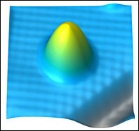
Scanning tunneling microscope topograph of an iron atom (yellow bump) on a nitride-covered substrate (blue) which may someday enable single-atom bit-cells for memory chips. Next to the iron atom is a one-atom-high step in the nitride surface (grey).
The technique could be a valuable tool to study solar cells, and quantum computing, and could also help explore whether or not information can be reliably stored on a single atom, the researchers said.
"There are several applications that we can look at now that we have this vast time-resolution atomic-scale spatial resolution," Heinrich said. "Of course, for us the most important one is electronic equipment -- processors work on the time scale of nanoseconds, and now we can look at processes on that time scale in real time and in real space. But there are many other applications, including, for example, solar technologies where we need to learn about the energy conversion of photons into electrons on the molecular scale."
"I am particularly excited by the possibility of generalizing it to other systems, such as photovoltaics, where a combination of high spatial and time resolution will help us to better understand various nanoscale processes important for solar energy, including light absorption and separation of charge," said Michael Crommie of the University of California, Berkeley, about the technique.
The research is published in the current issue of the journal Science.
For more information, visit: www.ibm.com
Published: September 2010