Chip features are small, and the defects that make them fail, even smaller. What is more, inspecting chips must be done on an assembly line, where throughput is crucial. Add to that layers of reflective and other obscuring films, and you have a recipe for a real challenge.
There is one other factor that must be considered. Because of technological advances, chip inspectors must hit a moving target, and their aim must be not on today’s technology or even tomorrow’s, but on that of the day after.
As Dilip Patel, defect metrology program manager at the International Sematech Manufacturing Initiative (ISMI), a chip manufacturing consortium in Austin, Texas, noted, “In general, you need metrology before any other technology.”
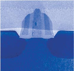
Advances in semiconductor manufacturing require that chips in production be inspected for new parameters such as strain, which could be done using x-ray diffraction of Raman spectroscopy. This image shows strained silicon, used to boost performance. Courtesy of ISMI and Intel.
Whereas today’s state-of-the-art semiconductors have minimum feature sizes in the 50-nm range, researchers already are worrying about defects two or three process nodes ahead. They are struggling to come up with reliable methods to detect defects with dimensions below 10 nm. Consequently, industry and academic researchers are seeking new ways – and new wavelengths – to inspect semiconductors. A survey shows some successes and outlines what remains to be done.
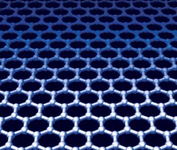
New semiconductor materials, such as the graphene shown here, will require new inspection metrology techniques. Candidates include x-ray diffraction, spectroscopic ellipsometry, and spectroscopic and x-ray reflectometry. Courtesy of Thomas Szkopek, McGill University.
The inspection challenge can be broken down into three phases: spotting point defects, measuring the thickness of films and determining critical dimensions, which are measurements of the sizes of important circuit pattern features.
Given the dozens of processing steps a chip goes through during fabrication and the need to sample a meaningful percentage of the hundreds of chips on a wafer, inspection speed is paramount. Much of today’s chip checks are done using optical tools, in part for historical reasons and in part because such an approach offers the required throughput.
Detecting invisible defects
With regard to the first inspection category, some tools operate with light in the ultraviolet to blue regions of the spectrum, or about 250 to 450 nm. The rule of thumb is that a killer defect can be as small as half the feature size of the circuitry. Because today’s state-of-the-art processes are at the 45-nm node, that means the tools are being used to spot something that is a little over 20 nm in size.
That is well below the classical resolution limit; thus, the defects cannot be resolved into discrete objects. But the situation isn’t anything new.
“Defects have been unresolved for more than five years and closer to a decade,” said Greg Kirk, vice president of technology for the optical patterned wafer inspection line of products at KLA-Tencor Corp. in Milpitas, Calif. The company makes a variety of chip inspection tools.
In describing the situation, Kirk said, “The defect shows up as a point-spread-functionlike dot. You’ve got to figure which dot is a defect and which is noise.”
The concept behind these optical inspection techniques is fairly straightforward: Hit the chip with light, make the defect interact with the light and collect the resulting signal for analysis. Over the years, KLA-Tencor has found that contrast is more important than resolution, and that images that look poor to the eye actually may be the best for defect detection. Thus, a longer wavelength – say around 450 nm – may yield better results than one in the ultraviolet.
Getting to that point, however, can require painstaking simulation work, with the various film layers and circuit geometry being used as parameters. Added to that must be factors such as line edge roughness, which can contribute to scatter and noise.
What will be needed in the future, Kirk said, are more powerful broadband light sources and more sensitive and speedy detectors. He noted that the company’s road map calls for sensors with data rates higher than 6.4 gigapixels per second, something not available today. On the optics front, it needs a broadband response with a wide field of view and a high numerical aperture in different illumination and collection sectors of the spectrum, he said. “That is key to collecting the signal we want and rejecting the noise we don’t.”
Nonoptical contenders
For its part, ISMI is working with vendors and researchers to facilitate the development of new inspection technologies. Doing so requires the creation of test structures that mimic the proposed stack of films that will make up tomorrow’s chips. Investigators then must create an array of defects of the right size and composition so that the inspection technology can be tested.
ISMI’s Patel noted that various approaches exist today that can do the job at larger defect sizes or at lower throughput. “The issue is to get smaller resolution and at the same time higher throughput.”
The consortium is working with FEI Co. of Hillsboro, Ore., maker of scanning electron microscopes, to improve that technology. Another area of investigation involves the helium-ion microscope supplied by Carl Zeiss SMT of Oberkochen, Germany.

Detecting defects in semiconductor chips may require the use of novel nonoptical methods as feature sizes shrink. Seen here are images obtained with a helium-ion microscope, a new inspection technology. Courtesy of Carl Zeiss.
As the name implies, the microscope uses a beam of helium ions. Because these ions weigh 8000 or so times what an electron does, they have a de Broglie wavelength that is about 300 times smaller. As a result, the beam suffers correspondingly less diffraction and can achieve a smaller spot size. It also can be used to characterize materials on the nanoscale, offering the prospect of enabling defect detection and classification in one tool.
Going to great lengths
Although nonphotonic methods are being pursued actively, don’t count out optical techniques. A case in point comes from research that appeared in the May 1, 2009, issue of Optics Letters. Lead author Edwin J. Heilweil, a chemist at the National Institute of Standards and Technology (NIST) in Gaithersburg, Md., said that the work began with the hope of imaging wafers for defects.
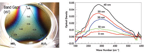
Terahertz measurements (left) of metal-oxide films reveal details on films as thin as 5 nm. On the right is a visible image of a mixed-oxide combinatorial library grown from yttrium, aluminum and hafnium targets. Courtesy of Edwin J. Heilweil, National Institute of Standards and Technology.
In its investigation, the NIST group modified a commercial IR detector, adding a beamsplitter and changing the sensor so that the device detected terahertz waves. Located between IR radiation and microwaves, terahertz waves can be used for a type of spectroscopy known to be very sensitive to crystal and molecular structures.
However, these wavelengths are 15 to 300 μm, roughly 1000 times the 50-nm-or-less thickness of the metal-oxide films being used in leading-edge semiconductors. Nonetheless, when the researchers looked at samples, they saw a large signal, one that changed when the crystalline phase of the film did. The technique yielded a useful signal from films as thin as 5 nm.
By way of explanation, Heilweil pointed to film vibration modes, or phonons. “These phonon modes in these types of materials are spread around the film, and they act like an antenna in a way.”
The phonon modes effectively increase the interaction cross section of the film, making a thin film yield the signal strength equivalent to a much thicker one. Before the technique can be used in production, more research and development must be done, particularly with regard to increasing the detected spectral bandwidth and spatial resolution. Heilweil believes that the use of the right laser as the light source can solve those problems.
Once bandwidth is sufficient, the method holds promise as an in-line film monitor because it can detect microscopic changes in the crystalline structure during deposition of titanium and hafnium and other metal-oxide films. The first two are in some of the latest semiconductors and are expected to be used much more extensively in next-generation devices.
Measuring the future
The NIST work illustrates that unusual wavelengths may prove unexpectedly useful, but new wavelengths also may present new problems. A case in point can be seen in thin-film metrology, which measures various film aspects.
Victor Vartanian, ISMI’s films metrology manager, noted that the industry faces some challenges because of transistor performance degradation that began when feature sizes went below 130 nm. Above that size, transistors gained in performance by going smaller; below, their performance suffered as they went smaller.
Regaining that lost performance has been possible through novel transistor engineering, but that, in turn, has made it necessary to measure the strain and other previously nonessential parameters in films. These measurements must be made on films that are sometimes only tens of nanometers thick.
This requirement has been met by the use of deep-UV or vacuum-UV. Consequently, there has been a need for different sources, detectors and optics. However, such energetic photons can raise new questions, Vartanian said. “What types of damage might you be doing to thin dielectric surfaces, and are you accounting for these effects?”
These questions could become more acute. One issue with x-ray and UV inspection has been the lack of high fluence sources. Increasing throughput can require brighter sources, but those same sources could adversely affect the films being inspected. Balancing throughput and yield could take considerable research and development.
The final aspect of chip inspection – critical dimensions – has long been measured via an optical technique called scatterometry. In it, light of a wavelength well above the feature size is scattered off chip structures, and the size of those features is then deduced from the scattering profile.
Solving the scattering problem with a two-dimensional model of the actual shape was sufficient in the past, said ISMI critical dimension project manager Benjamin Bunday, but now the 3-D shape of the structure must be taken into account. That change has meant that 15 or so parameters must go into the solution, instead of the five used previously. Some of the new ones involve the slope of the walls or the roughness of the edges of the features.
Of course, scatterometry has its limits. Investigators at NIST and ISMI have attempted to determine these, and their results indicate problems ahead, Bunday said. “With optical scatterometry, about the 22-nm node or the 18-nm node, you might see some issues. That’s when things will get interesting.”
However, he added, “Don’t say that’s set in stone. Suppliers will probably rally to the cause, as they have in the past, and find a way to make things work.”
In case they don’t, researchers are looking into an x-ray version of scatterometry. Putting it into production, however, requires an improvement of three orders of magnitude in source brightness and detector performance.
Going up
Another factor in the inspection challenge arises because the future of chips is looking up – literally. The latest twist is stacking chips atop one another in a 3-D structure. This is being done because of an ongoing need to route ever-faster signals around ever-larger chips through ever-smaller metal traces. Exploiting the third dimension gets around those problems, upping the performance and density of future chips.
However, it does add a new aspect – again literally – to the inspection challenge. The through-silicon vias that connect one stacked circuit to another stretch through the substrate, a distance that can run hundreds of microns for a full-size wafer and some fraction of that for a thinned one. Yet the vias themselves measure only, at most, a few tens of microns across. Thus, the aspect ratio – the depth divided by the width – can run as high as 15:1. It isn’t enough for the via just to reach the other side; the slope and shape of the walls also are important.
The inspection and stacking are done after the chips are largely finished. This means that a lot of money has been invested in them, and it is difficult to see through all of the film layers.
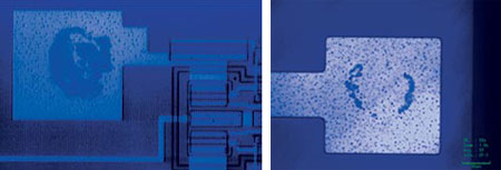
Near-IR inspection can detect details and defects not visible otherwise, particularly since silicon is transparent to near-IR. The image on the right is from a standard microscope equipped with near-IR, while the one on the left is from a high-resolution laser confocal microscope. Courtesy of Olympus America.
One possible solution being investigated is the use of near-IR, using wavelengths out to as much as 1700 nm, and an indium gallium arsenide camera as a detector. Olympus America Inc. of Center Valley, Pa., manufactures a microscope with near-IR imaging capabilities that could be used for this. With the near-IR approach, the alignment of the chips could be checked before the 3-D structure was finalized.
Linda Sikel, a product manager for Olympus America, noted that the key is being able to use wavelength, optics, sensors and image-forming techniques to make the job easier. Such optimization also is important for virtually any other optical inspection of semiconductors.
As for applying the right light to this particular inspection task, Sikel said, “What’s extremely valuable is the ability to see through the silicon.”