JACK JEWELL
Our VCSEL (vertical-cavity surface-emitting laser) project stemmed from my doctoral work, under Hyatt Gibbs between 1980 and 1984 at the University of Arizona Optical Sciences Center, using nonlinear optical properties of GaAs (gallium arsenide) to make all-optical logic gates that might be used in an optical computer. While the devices could also lase1, they would require more power, so we focused on gating. In 1984, I left Arizona for AT&T Bell Laboratories and, in the Optical Computing Research Department headed by Alan Huang, I continued the work I’d begun.
Thursday, May 11, 1989
"It was the first test of our first attempt to fabricate VCSELs. They lit up! Thousands of VCSELs on a crumb-size chip lased readily with low threshold currents (1s of mA), the smallest lasers in the world. The original ~6- × 8-mm2 chip held over a million of them. It was hard to fathom, especially since we’d never before designed or built a diode laser. Seasoned laser experts had laughed at our audaciousness and scorned our intercompany collaboration. But this experiment set the course for VCSEL research, development, and commercialization for more than 30 years, and for the foreseeable future."
— Jack Jewell, Axel Scherer, Sam McCall, Yong-Hee Lee, Jim Harbison, and Leigh Florez
A viable optical device would require the smallest possible size, density, and thickness (thus mirror reflectivities
>99%). Sam McCall of Bell Labs suggested growing an all-GaAs/AlAs (aluminum arsenide) distributed-feedback structure grown by molecular beam epitaxy (MBE), then etching the layers into vertical waveguiding “posts.” I preferred a resonator structure, with the active material sandwiched between passive mirrors. Our initial design would have both. Quickly grown at Bell in early 1986 by Art Gossard and John English, our structure showed optical gating.
For the next year, I tried to get researchers at Bell to etch the posts, or “microresonators,” but was unsuccessful; my requests were rebuffed for technical or other reasons. Finally, despite the political incorrectness, I contacted Axel Scherer at Bell Communications Research (Bellcore), a separate company. In short order, Axel etched the microresonators, as small as 1.5 µm across, on 3-µm pitch, and >4 µm deep. They gated excellently, were visually captivating, and the publications2 were well received. Thus began our intercompany collaboration
in early 1987.
Over the next couple years, Axel etched microresonators to sub-1/2-µm diameters,
and the microresonators revealed fascinating results. Yong-Hee Lee (also from Hyatt’s group) joined us at Bell, collaborated on microresonators, and initiated a project on resonator-based electro-optic modulators. Jim Harbison, a Bellcore MBE grower, became interested. He and Leigh Florez grew resonators with 99% reflectance for me, and modulator structures for Yong.
The prospect of optical computers based on our devices became increasingly elusive. Since our devices could lase, Sam and Yong encouraged laser investigations.
With optical pumping, structures with GaAs/AlAs mirrors and ~60 InGaAs quantum-well (QW) active regions lased readily, as did our older microresonators. Still, I was driven by the ultimately small embodiment: a single-QW (SQW) VCSEL.
In an early 1989 spontaneous collaboration, Kai Huang (Bell, MBE) grew VCSELs that had 60 QWs, then 20, then nine (in three intensity peaks, “periodic gain” à la Larry Coldren) then three QWs in a single peak, and finally an SQW. Yong and I achieved optically pumped ~980 nm lasing from all in about one week3. Audiences were surprised this was possible. Then we turned to our real goal: electrically pumped VCSELs.
Our all-semiconductor microresonator VCSELs required current flow through a GaAs/AlAs-based p-type mirror. Yong had seen that high resistance in his modulators’ p-mirrors prevented significant current flow because of the GaAs/AlAs well/barrier interfaces. Initially stumped, I found a publication showing that a graded superlattice reduced resistance at a single interface, so I resolved to incorporate these throughout the p-mirror interfaces. Sam and I designed a three-QW VCSEL with 504 layers in March 1989.
The 0.024-µm active region permitted a thin p-i-n junction and low current density, similar to those of highly successful edge-emitting lasers, and far unlike any prior VCSELs. Axel architected a one-etch process with emission through the GaAs substrate and a gold-top electrode, which I incorporated into the top mirror. Simplicity and low visibility were ideal for our quiet collaboration. In 1989, MBE growth changed material compositions via manual shutters. I was told the graded superlattices wouldn’t work and that no one would grow the 504-layer structure. Undaunted, Leigh and Jim grew them, exemplifying MBE (“many boring evenings”).
Axel evaporated gold over pieces of the wafer. I lithographically patterned the 1- to 5-µm devices, then evaporated chromium dots through the resulting holes for use as a mask. Axel etched the microresonator VCSELs, and then took the iconic scanning electron micrograph in the wee hours of May 11, while I observed and heckled. Later that morning, Yong and I silver-epoxied a corner of a smaller piece onto a glass slide, then contacted the tops of the 1- to 5-µm-diameter microlasers with a sharp electrical probe.
They lased as soon as we could test them. We spun a micrometer knob, raking a dozen VCSELs under the probe per second, and watched them blink on and off. We were mesmerized. All our team came to witness and revel. They lased up to ~30% duty cycle. We followed up with an SQW VCSEL, which performed similarly. Yong tried larger devices, 5 to 10 µm across and etched only halfway down. Improved heat dissipation resulted in room-temperature continuous-wave (RTCW) operation, which solidified our announcement4.
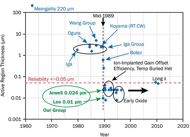
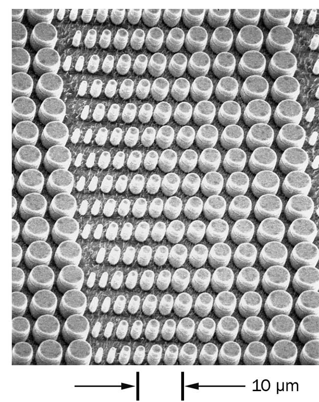
(Top) Each point corresponds to a publication of electrically pumped VCSELs. Ivar Melngailis’ 1965 device was 220 µm thick. Kenichi Iga and his group demonstrated electrically pumped VCSELs in 1979, described their advantages, led advancements through the 1980s, and achieved RTCW lasing in late 1988, with a 2.5-µm active region. In 1989, our collaboration introduced thin (~0.024 µm), practical active regions. See references 4-8. Jack Jewell, courtesy of Axel Scherer.
The chart of VCSEL active-material thickness versus time shows the sharp (50 to 100×) transition to viable structures initiated by our work. For low threshold and high reliability, and to fit within a single peak of standing-wave intensity, the thickness must be small (~0.05 µm or less), like commercial edge-emitting lasers, and VCSELs ever since. The features we introduced in 1989 (thin active region, mirror reflectivity >99%, graded-interface semiconductor mirrors, and semiconductor cavity) became the norm, and still comprise essentially all commercial VCSELs today.
Following our announcement, VCSEL R&D ramped quickly in academia and industry. Multiple groups made more
advancements with the new embodiments, including ion-implanted VCSELs (the first VCSEL product, the workhorse of the Gigabit Ethernet), gain-offset for temperature stability (still used in all VCSELs), and later, the oxide-confined VCSEL.
The three ingredients that enabled these breakthroughs: optics, collaboration, and risk.
Meet the author
Jack Jewell, Ph.D., led fundamental VCSEL advancements at Bell Laboratories (1984-1991). He co-founded Photonics Research (1991), founded Picolight (1995), furthered VCSEL technology throughout, and holds 74 U.S. patents. He received a doctorate in optical sciences in 1984 from the University of Arizona.
References
1. A. Passner et al. (1980). Ultrashort laser:
lasing in MBE GaAs layer with perpendicular-to-film optical excitation and emission. IEEE J. Quantum Electron, QE-16, Vol. 12, pp. 1283-1285.
2. J.L. Jewell et al. (1987). GaAs-AlAs monolithic microresonator arrays. Appl Phys Lett, Vol. 51, No. 2, pp. 94-96.
3. J.L. Jewell et al. (March 1-3, 1989). Vertical cavity single quantum well laser. OSA Proc Photonic Switching, Vol. 3, pp. 7-11, Postdeadline PD3.
4. J.L. Jewell et al. (July 19, 1989). Proc. Integrated Optics and Optical Fiber Communication Conf. IOOC ’89, Postdeadline paper 18B2-6.
5. I. Melngailis (1965). Longitudinal injection-plasma laser of InSb. Appl Phys Lett, Vol. 6, No. 3, pp. 59-60.
6. H. Soda et al. (1979). GaInAsP/InP surface emitting injection lasers. Jpn J Appl Phys, Vol. 18, No. 12, pp. 2329-2330.
7. J.L. Jewell et al. (Aug. 17, 1989). Low-threshold electrically pumped vertical-cavity surface-emitting microlasers. Electron Lett, Vol. 25, No. 17, pp. 1123-1124.
8. Y.H. Lee et al. (Sept. 28, 1989). Room-temperature continuous-wave vertical-cavity single-quantum-well microlaser diodes. Electron Lett, Vol. 25, No. 20, pp. 1377-1378.
Editor’s note: This sidebar came about as the result of a conversation following the December 2018 cover story, “Low-Powered VCSELs Find a Wide Variety of Uses.”