Invisibility cloaks get all the publicity, but they may just be the beginning if the promise
of transformation optics can be realized. The discipline could lead to smaller photonic
and electronic devices and more cost-competitive solar cells – in addition
to those long-sought-after invisibility cloaks.
Achieving these and other advances assumes that the challenges
confronting transformation optics can be successfully overcome. Chief among these
are dealing with losses and building the tiny structures needed in metamaterials,
the composite materials that make the field possible.
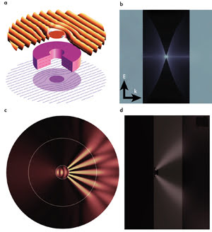
Transformation optics could be used to create
(a) an invisibility cloak, (b) a light concentrator or (c and d) a hyperlens. These
applications depend on steering light where desired: around an object for invisibility
or to a point for a concentrator. Courtesy of Vladimir M. Shalaev, Purdue University.
Taking the shortest path
Transformation optics work by exploiting how light travels, researcher
Vladimir M. Shalaev said. “Light propagates in such a way that it minimizes
the optical path, which is a product of the geometrical path and the refractive
index.”
Shalaev, a professor of electrical and computer engineering at
Purdue University in West Lafayette, Ind., is a key player in the new field. He
noted that bulk homogeneous materials have a single refractive index. Thus, the
path of light through them is determined by geometry.
Metamaterials, in contrast, can have a varying refractive index.
This can be done by building rings and rods, by embedding metallic nanoparticles
or by other means. The key is that the structures must be much smaller than the
wavelength of the light of interest and that the structures must interact with the
photons.
The result is an apparent refractive index at specific wavelengths
that is not restricted to being more than 1, as is the case with bulk materials.
Instead, it can be less, with values close to 0 and even negative possible.
Because of this, light then can be made to curve around objects,
which is how an invisibility cloak would work. It can be made to disappear into
a concentrator, never to re-emerge. It can even be made to reverse direction, all
courtesy of metamaterials with the right refractive index value and profile.
For Shalaev, the physics behind this is exciting, but he acknowledges
that applications ultimately will drive funding and the field itself. He noted ongoing
announcements of advances in invisibility cloaking and pointed out that making an
object look like something else has been demonstrated, which is a step toward cloaking.
Such mimicry can be beneficial when trying to hide something and is of interest
to the military.
But cloaking and mimicry are not where some of the first important
uses could arise, Shalaev said. “One of the first key applications of metamaterials
and transformation optics I expect to be in the area of subdiffraction imaging.
The most promising thing here is a planar magnifying hyperlens.”
Such a hyperlens would magnify objects that were below the traditional
diffraction limit, about a half-wavelength of light, so that they could be imaged
with conventional optics. A researcher using a standard microscope equipped with
a hyperlens could observe objects currently too small to see.
Just as importantly, a hyperlens would work in the opposite direction,
concentrating light into spots smaller than can be achieved with standard optics.
That capability could be of critical importance to the semiconductor industry, which
manufactures chips using nonlinear optical-based processing. That will be the basis
for the 22-nm technology node, expected to debut in 2011, but trouble looms beyond
that for the current 193-nm immersion lithography. A hyperlens would allow the extension
of current tricks to even smaller features and could be a boon to the chip industry.
Let the sun shine in
Besides a hyperlens, another potential transformation optics application
involves solar cells. Most are built using crystalline silicon wafers with a thickness
of up to 300 μm. That distance is required to efficiently capture the red part
of the spectrum, which is poorly absorbed by silicon.
However, silicon adds significantly to the cost of solar cells.
It is part of the reason why solar power is anywhere from two to five times as pricey
as it would have to be to be cost-competitive.
Transformation optics offers a solution to this problem through
the construction of plasmonic solar cells. These use metallic nanostructures that
support surface plasmons, excitations of the conduction electrons at the interface
between a metal and a dielectric. Properly engineered, these metallic-dielectric
structures can concentrate and fold the light into the semiconductor layer, making
possible more cost-effective solar cells.
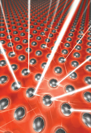
A plasmonic solar cell, shown in this artist’s rendering, at left, could cut the cost
of solar power. Light is scattered and trapped using an array of metal nanoparticles
placed either in front or in back of the solar cell. Less silicon is then needed.
Courtesy of AMOLF/Tremani.
“Plasmonic solar cells have the potential to make solar
cells ten to twenty times thinner, while keeping the efficiency the same. Because
materials costs constitute a large price of the solar cell, the needed two- to fivefold
reduction in price is within reach,” said Albert Polman, scientific group
leader at the FOM Institute for Atomic and Molecular Physics in Amsterdam, the Netherlands.
A pioneer in the plasmonic solar cell field, Polman said that
research results are encouraging. The addition of the metallic nanoparticles does
add to the cost of the solar cell, partly because the material of choice is silver
or gold. The cost, however, is minimal because the structures measure in the 100-nm
range.
There is also some added cost resulting from additional processing.
There are solutions to this issue, however. For example, Polman’s group has
developed a technique that allows the nanostructures to be added in a roll-to-roll
soft imprinting process to the back of the solar cell.
The current state of affairs, Polman explained, is that the concepts
have been proved in the lab, and the results agree with what models predict. It
is now a question of implementing a solution tailored to a particular solar cell
manufacturing process and showing the benefit in a real-world installation. He reported
that his group is working with manufacturers to do just that.
Kylie R. Catchpole, a research fellow at the Canberra-based Australian
National University, is an active collaborator of Polman’s. She noted that
one knob that researchers can turn to boost performance involves adjusting the plasmon
resonance, the wavelength of maximum photon interaction and scattering.
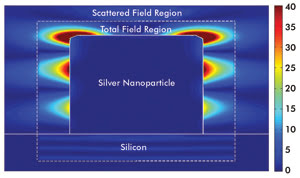
Standing waves form around a tall silver nanoparticle on a silicon substrate when light comes from
above. Such nanoparticles scatter more light into the silicon, making it absorb like a much thicker sample. Courtesy of Kylie R. Catchpole, Australian National University.
“There is much more scope for tuning the plasmon resonance
than we realized. This makes it very easy to make the scattering strongest in the
part of the spectrum where absorption most needs improving,” she said.
The overall behavior of the nanoparticles is strongly dependent
on their size, shape and arrangement, she added. Thus, fabrication techniques, as
well as design and characterization strategies, will be important in producing these
plasmonic solar cells.
Dealing with loss
There are some problems to be overcome, however, before a hyperlens,
plasmonic solar cell or an invisibility cloak can be built. One is manufacturing.
Because the metamaterials must have features well below the wavelength of the light
of interest, the structures involved can be quite small.
For the visible range of 400 to 700 nm, the dimensions may have
to be much less than 100 nm. That is one reason why so many demonstrations are done
first using microwaves. The longer wavelength means that the structures can be much
larger and, therefore, easier to construct.
Progress in this area is being made, however. Shalaev’s
group at Purdue, for instance, has made metamaterials with a negative refractive
index at 500 nm, well into the visible. Negative refraction is possible for only
a relatively narrow spectral window, but Shalaev pointed out that going negative
is not necessary for many applications. For these, the refractive index need only
be near 0 or vary between 0 and 1. Because of that, broadband use of transformation
optics is possible.
Another problem is optical loss. As photons traverse a metamaterial,
they can disappear into it. For some applications, that is not an issue. For others,
it can be a killer. An invisibility cloak that hides you but that looks black because
of light loss, for instance, wouldn’t be of much use.
There are solutions. One that has been proposed is to compensate
for the loss by adding something like dye molecules or quantum dots to the dielectric.
These would create optical gain, potentially negating any loss.
Such a scheme would have to be done carefully, cautioned Mikhail
A. Noginov, a professor of physics at Norfolk State University in Virginia. Too
much gain could lead to nonlinear effects and, with feedback, could result in a
laser. The goal would be to balance gain and loss, with the outcome a small loss.
Noginov also has done work in which the loss was reduced without
gain by alloying two metals together. In another loss-reducing scheme, he modified
the surface of a metal with dye molecules, which led to elongation of the surface
plasmon polariton propagation length. Both of these approaches, however, have their
own issues. The first, for instance, helps only at some wavelengths and actually
makes loss higher at others.
But, in speaking about the future, Noginov predicts that the loss
issue will be resolved. He said that silicon today is a nearly perfect material,
but this came only after decades of work. That history gives hope for tomorrow’s
transformation optics applications and the metamaterials that make them possible.
Speaking of the metamaterials, Noginov said, “Now they’re
not as good as we want, but probably after some time and some effort, they may be
significantly improved.”