Researchers at Brown University have developed an approach to scattering-type scanning near-field microscopy (s-SNOM) that uses blue light to enable measurement of electrons in semiconductors, as well as other nanoscale materials. The findings, which the researchers said are a first in nanoscale imaging, provide a workaround to a long-standing problem that has limited the study of key phenomena in a variety of materials that could one day lead to more energy-efficient semiconductors and electronics.
Coupling terahertz optical techniques to s-SNOM has recently emerged as a valuable new paradigm for probing nanoscale material properties on the nanoscale, the researchers said. To this end, researchers have previously demonstrated and effectively used techniques such as terahertz nanoscopy, nanoscale terahertz emission spectroscopy, and others.
However, according to the researchers, as with nearly all examples of s-SNOM since its development in the mid-1990s, the wavelength of the optical source coupled to the near-field tip is considered long, usually at energies of 2.5 eV or less. s-SNOM involves scattering light from a sharpened tip that is only a few tens of nanometers across. The tip hovers just above the sample material to be imaged. When the sample is illuminated, the light scatters and a portion of the scattered light is left with information about the nanosize region of the sample directly beneath the tip. That scattered radiation is analyzed so that information about the small volume of material can be extracted.
For wide bandgap materials such as silicon and gallium nitride, the challenge of coupling of shorter wavelengths such as blue lightwaves to the nanotip has inhibited the study of nanoscale phenomena, the researchers said.
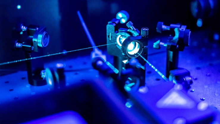
A team of Brown University researchers created a solution to a nanoscale resolution challenge that has for decades limited the study of materials that could lead to more energy efficient semiconductors and electronics. Courtesy of Brown University.
In the current experiment, the researchers used blue light to get measurements from a silicon sample that cannot be obtained using red light. The measurements provided a proof-of-concept about the use of shorter wavelengths to study materials on the nanoscale. “We were able to compare these new measurements to what one might expect to see from silicon, and the match was very good,” said Daniel Mittleman, a professor in Brown’s School of Engineering and author of the paper describing the work.
The researchers used the blue light to not only illuminate the sample so that the light scatters, but also to produce a burst of terahertz radiation from the sample. The radiation carries important information about the sample’s electrical properties, and though the solution adds an extra step and increases the amount of data that the scientists have to analyze, it eliminates the need to be as precise in how they align the tip over the sample.
According to the researchers, because the terahertz radiation has a much longer wavelength, it is much more easily aligned. “It still has to be really close, but it doesn’t have to be as close,” Mittleman said. “When you hit it with the light, you’ll still be able to get information in the terahertz.”
The researchers plan to use the technique to gain better insights into semiconductors used to produce blue LED technology.
The work was supported by the National Science Foundation Division of Electrical Communications and Cyber Systems, the Kansas City National Security Campus, and the Department of Energy.
The research was published in Light: Science & Applications (www.doi.org/10.1038/s41377-023-01137-y).